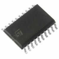
ST72F623F2M1 STMicroelectronics, ST72F623F2M1 Datasheet - Page 128

ST72F623F2M1
Manufacturer Part Number
ST72F623F2M1
Description
IC MCU 8BIT LS 8K 20-SOIC
Manufacturer
STMicroelectronics
Series
ST7r
Datasheet
1.ST72F622L2M1.pdf
(139 pages)
Specifications of ST72F623F2M1
Core Processor
ST7
Core Size
8-Bit
Speed
8MHz
Connectivity
USB
Peripherals
DMA, LVD, POR, PWM, WDT
Number Of I /o
11
Program Memory Size
8KB (8K x 8)
Program Memory Type
FLASH
Ram Size
384 x 8
Voltage - Supply (vcc/vdd)
4 V ~ 5.5 V
Data Converters
A/D 3x10b
Oscillator Type
Internal
Operating Temperature
0°C ~ 70°C
Package / Case
20-SOIC (7.5mm Width)
Processor Series
ST72F6x
Core
ST7
Data Bus Width
8 bit
Data Ram Size
384 B
Interface Type
SCI, SPI, USB
Maximum Clock Frequency
12 MHz
Number Of Programmable I/os
11
Number Of Timers
2
Operating Supply Voltage
4 V to 5.5 V
Maximum Operating Temperature
+ 70 C
Mounting Style
SMD/SMT
Minimum Operating Temperature
0 C
On-chip Adc
10 bit
Lead Free Status / RoHS Status
Contains lead / RoHS non-compliant
Eeprom Size
-
Lead Free Status / Rohs Status
Details
Other names
497-2114-5
Available stocks
Company
Part Number
Manufacturer
Quantity
Price
Company:
Part Number:
ST72F623F2M1
Manufacturer:
NXP
Quantity:
670
Part Number:
ST72F623F2M1
Manufacturer:
ST
Quantity:
20 000
14 DEVICE CONFIGURATION AND ORDERING INFORMATION
Each device is available for production in user pro-
grammable versions (FLASH) as well as in factory
coded versions (ROM).
ST7262 devices are ROM versions.
ST72F62 FLASH devices are shipped to custom-
ers with a default content (FFh). This implies that
FLASH devices have to be configured by the cus-
tomer using the Option Byte while the ROM devic-
es are factory-configured.
14.1 OPTION BYTE
The Option Byte allows the hardware configuration
of the microcontroller to be selected.
The Option Byte has no address in the memory
map and can be accessed only in programming
mode using a standard ST7 programming tool.
The default content of the FLASH is fixed to FFh.
This means that all the options have “1” as their
default value.
Bits 7:6 = Reserved.
Bit 5 = WDGSW Hardware or software watchdog
This option bit selects the watchdog type.
0: Hardware enabled
1: Software enabled
Bit 4 = NEST
14.2 DEVICE ORDERING INFORMATION AND TRANSFER OF CUSTOMER CODE
Customer code is made up of the ROM contents
and the list of the selected options (if any). The
ROM contents are to be sent on diskette, or by
electronic means, with the hexadecimal file in .S19
format generated by the development tool. All un-
used bytes must be set to FFh.
128/139
7
-
-
WDG
SW
NEST LVD
-
OSC
12/6
FMP_
R
0
Doc ID 6996 Rev 5
This option bit selects the nested interrupts fea-
ture.
0: Nested interrupt feature disabled
1: Nested interrupt feature enabled
Bit 3 = LVD Low Voltage Detector selection
This option bit selects the LVD.
0: LVD enabled
1: LVD disabled
Bit 2= Reserved.
Bit 1 = OSC12/6 Oscillator selection
This option bit selects the clock divider used to
drive the USB interface at 6MHz.
0: 6 MHz oscillator (no divider for USB)
1: 12 Mhz oscillator (2 divider for USB)
Bit 0 = FMP_R Memory Readout Protection
Readout protection, when selected provides a pro-
tection against program memory content extrac-
tion and against write access to Flash memory.
Erasing the option bytes when the FMP_R option
is selected will cause the whole memory to be
erased first and the device can be reprogrammed.
Refer to the ST7 Flash Programming Reference
Manual and
tails.
0: Read-out protection enabled
1: Read-out protection disabled
The selected options are communicated to STMi-
croelectronics using the correctly completed OP-
TION LIST appended.
Refer to application note AN1635 for information
on the counter listing returned by ST after code
has been transferred.
The STMicroelectronics Sales Organization will be
pleased to provide detailed information on con-
tractual points.
section 4.3.1 on page 14
for more de-


