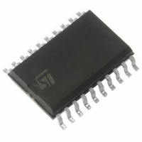
ST72F623F2M1 STMicroelectronics, ST72F623F2M1 Datasheet - Page 91

ST72F623F2M1
Manufacturer Part Number
ST72F623F2M1
Description
IC MCU 8BIT LS 8K 20-SOIC
Manufacturer
STMicroelectronics
Series
ST7r
Datasheet
1.ST72F622L2M1.pdf
(139 pages)
Specifications of ST72F623F2M1
Core Processor
ST7
Core Size
8-Bit
Speed
8MHz
Connectivity
USB
Peripherals
DMA, LVD, POR, PWM, WDT
Number Of I /o
11
Program Memory Size
8KB (8K x 8)
Program Memory Type
FLASH
Ram Size
384 x 8
Voltage - Supply (vcc/vdd)
4 V ~ 5.5 V
Data Converters
A/D 3x10b
Oscillator Type
Internal
Operating Temperature
0°C ~ 70°C
Package / Case
20-SOIC (7.5mm Width)
Processor Series
ST72F6x
Core
ST7
Data Bus Width
8 bit
Data Ram Size
384 B
Interface Type
SCI, SPI, USB
Maximum Clock Frequency
12 MHz
Number Of Programmable I/os
11
Number Of Timers
2
Operating Supply Voltage
4 V to 5.5 V
Maximum Operating Temperature
+ 70 C
Mounting Style
SMD/SMT
Minimum Operating Temperature
0 C
On-chip Adc
10 bit
Lead Free Status / RoHS Status
Contains lead / RoHS non-compliant
Eeprom Size
-
Lead Free Status / Rohs Status
Details
Other names
497-2114-5
Available stocks
Company
Part Number
Manufacturer
Quantity
Price
Company:
Part Number:
ST72F623F2M1
Manufacturer:
NXP
Quantity:
670
Part Number:
ST72F623F2M1
Manufacturer:
ST
Quantity:
20 000
10.7 10-BIT A/D CONVERTER (ADC)
10.7.1 Introduction
The on-chip Analog to Digital Converter (ADC) pe-
ripheral is a 10-bit, successive approximation con-
verter with internal sample and hold circuitry. This
peripheral has up to 8 multiplexed analog input
channels (refer to device pin out description) that
allow the peripheral to convert the analog voltage
levels from up to 8 different sources.
The result of the conversion is stored in a 10-bit
Data Register. The A/D converter is controlled
through a Control/Status Register.
10.7.2 Main Features
■
■
■
■
■
■
■
The block diagram is shown in
10.7.3 Functional Description
10.7.3.1 Analog Power Supply
Depending on the MCU pin count, the package
may feature separate V
er supply pins. These pins supply power to the A/D
converter cell and function as the high and low ref-
erence voltages for the conversion. In smaller
packages V
and the analog supply and reference pads are in-
ternally bonded to the V
Separation of the digital and analog power pins al-
low board designers to improve A/D performance.
Conversion accuracy can be impacted by voltage
drops and noise in the event of heavily loaded or
badly decoupled power supply lines.
10.7.3.2 PCB Design Guidelines
To obtain best results, some general design and
layout rules should be followed when designing
the application PCB to shield the noise-sensitive,
analog physical interface from noise-generating
CMOS logic signals.
– Use separate digital and analog planes. The an-
alog ground plane should be connected to the
10-bit conversion
Up to 8 channels with multiplexed input
Linear successive approximation
Data register (DR) which contains the results
Conversion complete status flag
Continuous or One-Shot mode
On/off bit (to reduce consumption)
DDA
and V
SSA
DDA
DD
and V
pins are not available
and V
Figure
SS
SSA
pins.
analog pow-
52.
Doc ID 6996 Rev 5
– Filter power to the analog power planes. The
– Properly place components and route the signal
10.7.3.3 Digital A/D Conversion Result
The conversion is monotonic, meaning that the re-
sult never decreases if the analog input does not
and never increases if the analog input does not.
If the input voltage (V
(high-level voltage reference) then the conversion
result is FFh in the ADCDRMSB register and 03h
in the ADCDRLSB register (without overflow indi-
cation).
If the input voltage (V
level voltage reference) then the conversion result
in the ADCDRMSB and ADCDRLSB registers is
00 00h.
The A/D converter is linear and the digital result of
the conversion is stored in the ADCDRMSB and
ADCDRLSB registers. The accuracy of the con-
version is described in the Electrical Characteris-
tics Section.
R
for an analog input signal. If the impedance is too
high, this will result in a loss of accuracy due to
leakage and sampling not being completed in the
allotted time.
digital ground plane via a single point on the
PCB. The analog power plane should be con-
nected to the digital power plane via an RC net-
work.
best solution is to connect a 0.1µF capacitor, with
good high frequency characteristics, between
V
to the V
log and digital power supplies in a star network.
Do not use a resistor, as V
ence voltage by the A/D converter and resist-
ance would cause a voltage drop and a loss of
accuracy.
traces on the PCB to shield the analog inputs.
Analog signals paths should run over the analog
ground plane and be as short as possible. Isolate
analog signal from digital signals that may switch
while the analog inputs are being sampled by the
A/D converter. Do not toggle digital outputs on
the same I/O port as the A/D input being convert-
ed.
AIN
DDA
is the maximum recommended impedance
and V
DDA
SSA
and V
and place it as close as possible
SSA
AIN
AIN
pins and connect the ana-
) is lower than V
) is greater than V
DDA
is used as a refer-
SSA
91/139
(low-
DDA


