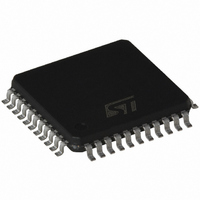
ST72F324J6T6 STMicroelectronics, ST72F324J6T6 Datasheet - Page 159

ST72F324J6T6
Manufacturer Part Number
ST72F324J6T6
Description
IC MCU 8BIT 32K 44-TQFP
Manufacturer
STMicroelectronics
Series
ST7r
Specifications of ST72F324J6T6
Core Processor
ST7
Core Size
8-Bit
Speed
8MHz
Connectivity
SCI, SPI
Peripherals
LVD, POR, PWM, WDT
Number Of I /o
32
Program Memory Size
32KB (32K x 8)
Program Memory Type
FLASH
Ram Size
1K x 8
Voltage - Supply (vcc/vdd)
3.8 V ~ 5.5 V
Data Converters
A/D 12x10b
Oscillator Type
Internal
Operating Temperature
-40°C ~ 85°C
Package / Case
44-TQFP, 44-VQFP
Controller Family/series
ST7
No. Of I/o's
32
Ram Memory Size
1KB
Cpu Speed
8MHz
No. Of Timers
2
Embedded Interface Type
SCI, SPI
No. Of Pwm Channels
1
Rohs Compliant
Yes
Processor Series
ST72F3x
Core
ST7
Data Bus Width
8 bit
Data Ram Size
1024 B
Interface Type
SCI, SPI
Maximum Clock Frequency
8 MHz
Number Of Programmable I/os
32
Number Of Timers
4 bit
Operating Supply Voltage
3.8 V to 5.5 V
Maximum Operating Temperature
+ 85 C
Mounting Style
SMD/SMT
Development Tools By Supplier
ST7F521-IND/USB, ST7232X-EVAL, ST7MDT20-DVP3, ST7MDT20J-EMU3, STX-RLINK
Minimum Operating Temperature
- 40 C
On-chip Adc
10 bit
Cpu Family
ST7
Device Core Size
8b
Frequency (max)
8MHz
Total Internal Ram Size
1KB
# I/os (max)
32
Number Of Timers - General Purpose
2
Operating Supply Voltage (typ)
5V
Operating Supply Voltage (max)
5.5V
Operating Supply Voltage (min)
3.8V
Instruction Set Architecture
CISC
Operating Temp Range
-40C to 85C
Operating Temperature Classification
Industrial
Mounting
Surface Mount
Pin Count
44
Package Type
TQFP
For Use With
497-8222 - UPS (LINE INTERACTIVE - 450W)497-8436 - BOARD EVAL UPS 450W VOUT=220V497-6421 - BOARD EVAL DGTL BATT CHGR DESIGN
Lead Free Status / RoHS Status
Contains lead / RoHS non-compliant
Eeprom Size
-
Lead Free Status / Rohs Status
In Transition
Other names
497-2108
Available stocks
Company
Part Number
Manufacturer
Quantity
Price
Company:
Part Number:
ST72F324J6T6
Manufacturer:
STMicroelectronics
Quantity:
10 000
Part Number:
ST72F324J6T6
Manufacturer:
ST
Quantity:
20 000
Company:
Part Number:
ST72F324J6T6/TR
Manufacturer:
STMicroelectronics
Quantity:
10 000
15 KNOWN LIMITATIONS
15.1 ALL DEVICES
15.1.1 External RC option
The External RC clock source option described in
previous datasheet revisions is no longer support-
ed and has been removed from this specification.
15.1.2 CSS Function
The Clock Security System function has been re-
moved from the datasheet.
15.1.3 Safe Connection of OSC1/OSC2 Pins
The OSC1 and/or OSC2 pins must not be left un-
connected otherwise the ST7 main oscillator may
start and, in this configuration, could generate an
f
maximum (>16MHz.), putting the ST7 in an un-
safe/undefined state. Refer to
24.
15.1.4 Unexpected Reset Fetch
If an interrupt request occurs while a “POP CC” in-
struction is executed, the interrupt controller does
not recognise the source of the interrupt and, by
default, passes the RESET vector address to the
CPU.
Workaround
To solve this issue, a “POP CC” instruction must
always be preceded by a “SIM” instruction.
15.1.5
interrupt routine
When an active interrupt request occurs at the
same time as the related flag is being cleared, an
unwanted reset may occur.
Note: clearing the related interrupt mask will not
generate an unwanted reset
Concurrent interrupt context
The symptom does not occur when the interrupts
are handled normally, i.e.
when:
– The interrupt flag is cleared within its own inter-
– The interrupt flag is cleared within any interrupt
– The interrupt flag is cleared in any part of the
If these conditions are not met, the symptom can
be avoided by implementing the following se-
quence:
Perform SIM and RIM operation before and after
resetting an active interrupt request.
OSC
rupt routine
routine
code while this interrupt is disabled
clock frequency in excess of the allowed
Clearing
active
interrupts
Section 6.2 on page
outside
Example:
Nested interrupt context:
The symptom does not occur when the interrupts
are handled normally, i.e.
when:
– The interrupt flag is cleared within its own inter-
– The interrupt flag is cleared within any interrupt
– The interrupt flag is cleared in any part of the
If these conditions are not met, the symptom can
be avoided by implementing the following se-
quence:
15.1.6 External Interrupt Missed
To avoid any risk of generating a parasitic inter-
rupt, the edge detector is automatically disabled
for one clock cycle during an access to either DDR
and OR. Any input signal edge during this period
will not be detected and will not generate an inter-
rupt.
This case can typically occur if the application re-
freshes the port configuration registers at intervals
during runtime.
Workaround
The workaround is based on software checking
the level on the interrupt pin before and after writ-
ing to the PxOR or PxDDR registers. If there is a
level change (depending on the sensitivity pro-
grammed for this pin) the interrupt routine is in-
voked using the call instruction with three extra
PUSH instructions before executing the interrupt
routine (this is to make the call compatible with the
IRET instruction at the end of the interrupt service
routine).
But detection of the level change does ensure that
edge occurs during the critical 1 cycle duration and
the interrupt has been missed. This may lead to
occurrence of same interrupt twice (one hardware
and another with software call).
rupt routine
routine with higher or identical priority level
code while this interrupt is disabled
SIM
reset interrupt flag
RIM
PUSH CC
SIM
reset interrupt flag
POP CC
ST72324Jx ST72324Kx
159/164
1


