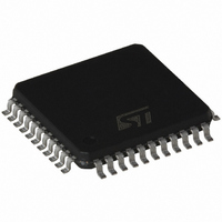
ST72F324J6T6 STMicroelectronics, ST72F324J6T6 Datasheet - Page 93

ST72F324J6T6
Manufacturer Part Number
ST72F324J6T6
Description
IC MCU 8BIT 32K 44-TQFP
Manufacturer
STMicroelectronics
Series
ST7r
Specifications of ST72F324J6T6
Core Processor
ST7
Core Size
8-Bit
Speed
8MHz
Connectivity
SCI, SPI
Peripherals
LVD, POR, PWM, WDT
Number Of I /o
32
Program Memory Size
32KB (32K x 8)
Program Memory Type
FLASH
Ram Size
1K x 8
Voltage - Supply (vcc/vdd)
3.8 V ~ 5.5 V
Data Converters
A/D 12x10b
Oscillator Type
Internal
Operating Temperature
-40°C ~ 85°C
Package / Case
44-TQFP, 44-VQFP
Controller Family/series
ST7
No. Of I/o's
32
Ram Memory Size
1KB
Cpu Speed
8MHz
No. Of Timers
2
Embedded Interface Type
SCI, SPI
No. Of Pwm Channels
1
Rohs Compliant
Yes
Processor Series
ST72F3x
Core
ST7
Data Bus Width
8 bit
Data Ram Size
1024 B
Interface Type
SCI, SPI
Maximum Clock Frequency
8 MHz
Number Of Programmable I/os
32
Number Of Timers
4 bit
Operating Supply Voltage
3.8 V to 5.5 V
Maximum Operating Temperature
+ 85 C
Mounting Style
SMD/SMT
Development Tools By Supplier
ST7F521-IND/USB, ST7232X-EVAL, ST7MDT20-DVP3, ST7MDT20J-EMU3, STX-RLINK
Minimum Operating Temperature
- 40 C
On-chip Adc
10 bit
Cpu Family
ST7
Device Core Size
8b
Frequency (max)
8MHz
Total Internal Ram Size
1KB
# I/os (max)
32
Number Of Timers - General Purpose
2
Operating Supply Voltage (typ)
5V
Operating Supply Voltage (max)
5.5V
Operating Supply Voltage (min)
3.8V
Instruction Set Architecture
CISC
Operating Temp Range
-40C to 85C
Operating Temperature Classification
Industrial
Mounting
Surface Mount
Pin Count
44
Package Type
TQFP
For Use With
497-8222 - UPS (LINE INTERACTIVE - 450W)497-8436 - BOARD EVAL UPS 450W VOUT=220V497-6421 - BOARD EVAL DGTL BATT CHGR DESIGN
Lead Free Status / RoHS Status
Contains lead / RoHS non-compliant
Eeprom Size
-
Lead Free Status / Rohs Status
In Transition
Other names
497-2108
Available stocks
Company
Part Number
Manufacturer
Quantity
Price
Company:
Part Number:
ST72F324J6T6
Manufacturer:
STMicroelectronics
Quantity:
10 000
Part Number:
ST72F324J6T6
Manufacturer:
ST
Quantity:
20 000
Company:
Part Number:
ST72F324J6T6/TR
Manufacturer:
STMicroelectronics
Quantity:
10 000
SERIAL COMMUNICATIONS INTERFACE (Cont’d)
10.5.4.2 Transmitter
The transmitter can send data words of either 8 or
9 bits depending on the M bit status. When the M
bit is set, word length is 9 bits and the 9th bit (the
MSB) has to be stored in the T8 bit in the SCICR1
register.
Character Transmission
During an SCI transmission, data shifts out least
significant bit first on the TDO pin. In this mode,
the SCIDR register consists of a buffer (TDR) be-
tween the internal bus and the transmit shift regis-
ter (see
Procedure
– Select the M bit to define the word length.
– Select the desired baud rate using the SCIBRR
– Set the TE bit to assign the TDO pin to the alter-
– Access the SCISR register and write the data to
Clearing the TDRE bit is always performed by the
following software sequence:
1. An access to the SCISR register
2. A write to the SCIDR register
The TDRE bit is set by hardware and it indicates:
– The TDR register is empty.
– The data transfer is beginning.
– The next data can be written in the SCIDR regis-
This flag generates an interrupt if the TIE bit is set
and the I bit is cleared in the CCR register.
When a transmission is taking place, a write in-
struction to the SCIDR register stores the data in
the TDR register and which is copied in the shift
register at the end of the current transmission.
When no transmission is taking place, a write in-
struction to the SCIDR register places the data di-
rectly in the shift register, the data transmission
starts, and the TDRE bit is immediately set.
and the SCIETPR registers.
nate function and to send a idle frame as first
transmission.
send in the SCIDR register (this sequence clears
the TDRE bit). Repeat this sequence for each
data to be transmitted.
ter without overwriting the previous data.
Figure
1.).
When a frame transmission is complete (after the
stop bit) the TC bit is set and an interrupt is gener-
ated if the TCIE is set and the I bit is cleared in the
CCR register.
Clearing the TC bit is performed by the following
software sequence:
1. An access to the SCISR register
2. A write to the SCIDR register
Note: The TDRE and TC bits are cleared by the
same software sequence.
Break Characters
Setting the SBK bit loads the shift register with a
break character. The break frame length depends
on the M bit (see
As long as the SBK bit is set, the SCI send break
frames to the TDO pin. After clearing this bit by
software the SCI insert a logic 1 bit at the end of
the last break frame to guarantee the recognition
of the start bit of the next frame.
Idle Characters
Setting the TE bit drives the SCI to send an idle
frame before the first data frame.
Clearing and then setting the TE bit during a trans-
mission sends an idle frame after the current word.
Note: Resetting and setting the TE bit causes the
data in the TDR register to be lost. Therefore the
best time to toggle the TE bit is when the TDRE bit
is set, that is, before writing the next byte in the
SCIDR.
Figure
ST72324Jx ST72324Kx
2.).
93/164
1


