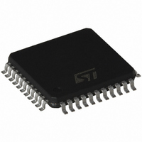
ST72F361J9T6 STMicroelectronics, ST72F361J9T6 Datasheet - Page 10

ST72F361J9T6
Manufacturer Part Number
ST72F361J9T6
Description
IC MCU 8BIT 60K FLASH 44-LQFP
Manufacturer
STMicroelectronics
Series
ST7r
Datasheet
1.ST72F361K6T6.pdf
(225 pages)
Specifications of ST72F361J9T6
Core Processor
ST7
Core Size
8-Bit
Speed
8MHz
Connectivity
LINSCI, SPI
Peripherals
LVD, POR, PWM, WDT
Number Of I /o
32
Program Memory Size
60KB (60K x 8)
Program Memory Type
FLASH
Ram Size
2K x 8
Voltage - Supply (vcc/vdd)
3.8 V ~ 5.5 V
Data Converters
A/D 16x10b
Oscillator Type
External
Operating Temperature
-40°C ~ 85°C
Package / Case
44-LQFP
Processor Series
ST72F3x
Core
ST7
Data Bus Width
8 bit
Data Ram Size
2 KB
Interface Type
LINSCI, SPI
Maximum Clock Frequency
8 MHz
Number Of Programmable I/os
34
Number Of Timers
2
Maximum Operating Temperature
+ 85 C
Mounting Style
SMD/SMT
Development Tools By Supplier
ST72F36X-SK/RAIS, STX-RLINK
Minimum Operating Temperature
- 40 C
On-chip Adc
10 bit, 11 Channel
Lead Free Status / RoHS Status
Lead free / RoHS Compliant
Eeprom Size
-
Lead Free Status / Rohs Status
Details
Available stocks
Company
Part Number
Manufacturer
Quantity
Price
Company:
Part Number:
ST72F361J9T6
Manufacturer:
STMicroelectronics
Quantity:
50
Company:
Part Number:
ST72F361J9T6
Manufacturer:
STMicroelectronics
Quantity:
10 000
- Current page: 10 of 225
- Download datasheet (8Mb)
ST72361
Notes:
1. In the interrupt input column, “eiX” defines the associated external interrupt vector. If the weak pull-up column (wpu) is
merged with the interrupt column (int), then the I/O configuration is pull-up interrupt input, else the configuration is floating
interrupt input.
2. Input mode can be used for general purpose I/O, output mode cannot be used.
3. OSC1 and OSC2 pins connect a crystal/ceramic resonator, or an external source to the on-chip oscillator; see
6
4. On the chip, each I/O port has eight pads. Pads that are not bonded to external pins are in input pull-up configuration
after reset. The configuration of these pads must be kept at reset state to avoid added current consumption.
10/225
54 36 26 PD4 / SCI2_RDI
55 37 27 V
56 38 28 V
57 39 29 V
58 40 30 V
59 41 31 PD5 / SCI2_TDO
60 42 32 RESET
61 43
62 44
63
64
and
Pin n°
Section 12.5 "CLOCK AND TIMING CHARACTERISTICS"
-
-
-
-
-
-
PD6 / AIN10
PD7 / AIN11
PF6
PF7
SSA
SS_0
DDA
DD_0
Pin Name
I/O C
I/O C
I/O C
I/O C
I/O C
I/O T
I/O T
S
S
S
I
Level
T
T
T
T
T
T
T
X
X
X
X
X
X
X
X
X
Input
ei3
ei3
ei3 X
Port
for more details.
X
Output
X
X
X
X
X
X
X
X
X
X
X
X
function
Port D4
Analog Ground Voltage
Digital Ground Voltage
Analog Reference Voltage for ADC
Digital Main Supply Voltage
Port D5
Top priority non maskable interrupt.
Port D6
Port D7
Port F6
Port F7
reset)
(after
Main
LINSCI2 Receive Data in-
put
LINSCI2 Transmit Data
output
ADC Analog Input 10
ADC Analog Input 11
Alternate function
Section
Related parts for ST72F361J9T6
Image
Part Number
Description
Manufacturer
Datasheet
Request
R

Part Number:
Description:
STMicroelectronics [RIPPLE-CARRY BINARY COUNTER/DIVIDERS]
Manufacturer:
STMicroelectronics
Datasheet:

Part Number:
Description:
STMicroelectronics [LIQUID-CRYSTAL DISPLAY DRIVERS]
Manufacturer:
STMicroelectronics
Datasheet:

Part Number:
Description:
BOARD EVAL FOR MEMS SENSORS
Manufacturer:
STMicroelectronics
Datasheet:

Part Number:
Description:
NPN TRANSISTOR POWER MODULE
Manufacturer:
STMicroelectronics
Datasheet:

Part Number:
Description:
TURBOSWITCH ULTRA-FAST HIGH VOLTAGE DIODE
Manufacturer:
STMicroelectronics
Datasheet:

Part Number:
Description:
Manufacturer:
STMicroelectronics
Datasheet:

Part Number:
Description:
DIODE / SCR MODULE
Manufacturer:
STMicroelectronics
Datasheet:

Part Number:
Description:
DIODE / SCR MODULE
Manufacturer:
STMicroelectronics
Datasheet:

Part Number:
Description:
Search -----> STE16N100
Manufacturer:
STMicroelectronics
Datasheet:

Part Number:
Description:
Search ---> STE53NA50
Manufacturer:
STMicroelectronics
Datasheet:

Part Number:
Description:
NPN Transistor Power Module
Manufacturer:
STMicroelectronics
Datasheet:

Part Number:
Description:
DIODE / SCR MODULE
Manufacturer:
STMicroelectronics
Datasheet:


