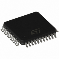
ST72F361J9T6 STMicroelectronics, ST72F361J9T6 Datasheet - Page 8

ST72F361J9T6
Manufacturer Part Number
ST72F361J9T6
Description
IC MCU 8BIT 60K FLASH 44-LQFP
Manufacturer
STMicroelectronics
Series
ST7r
Datasheet
1.ST72F361K6T6.pdf
(225 pages)
Specifications of ST72F361J9T6
Core Processor
ST7
Core Size
8-Bit
Speed
8MHz
Connectivity
LINSCI, SPI
Peripherals
LVD, POR, PWM, WDT
Number Of I /o
32
Program Memory Size
60KB (60K x 8)
Program Memory Type
FLASH
Ram Size
2K x 8
Voltage - Supply (vcc/vdd)
3.8 V ~ 5.5 V
Data Converters
A/D 16x10b
Oscillator Type
External
Operating Temperature
-40°C ~ 85°C
Package / Case
44-LQFP
Processor Series
ST72F3x
Core
ST7
Data Bus Width
8 bit
Data Ram Size
2 KB
Interface Type
LINSCI, SPI
Maximum Clock Frequency
8 MHz
Number Of Programmable I/os
34
Number Of Timers
2
Maximum Operating Temperature
+ 85 C
Mounting Style
SMD/SMT
Development Tools By Supplier
ST72F36X-SK/RAIS, STX-RLINK
Minimum Operating Temperature
- 40 C
On-chip Adc
10 bit, 11 Channel
Lead Free Status / RoHS Status
Lead free / RoHS Compliant
Eeprom Size
-
Lead Free Status / Rohs Status
Details
Available stocks
Company
Part Number
Manufacturer
Quantity
Price
Company:
Part Number:
ST72F361J9T6
Manufacturer:
STMicroelectronics
Quantity:
50
Company:
Part Number:
ST72F361J9T6
Manufacturer:
STMicroelectronics
Quantity:
10 000
- Current page: 8 of 225
- Download datasheet (8Mb)
ST72361
PIN DESCRIPTION (Cont’d)
For external pin connection guidelines, refer to
Legend / Abbreviations for
Type:
In/Output level: C
Output level:
Port and control configuration:
Refer to
The RESET configuration of each pin is shown in bold which is valid as long as the device is in reset state.
Table 2. Device Pin Description
8/225
10
11
12
13
14
15 10
16 11
17
18
19 12
20
21
22 13 10 PB5 / AIN1 / ICCDATA I/O C
– Input:
– Output:
1
2
3
4
5
6
7
8
9
Pin n°
1
2
3
4
5
6
7
8
9
-
-
-
-
-
-
-
-
-
“I/O PORTS” on page 45
1
2
3
4
5
6
7
8
9
-
-
-
-
-
-
-
-
-
-
-
-
OSC1
OSC2
PA0 / ARTIC1
PA1 / PWM0
PA2 (HS) / PWM1
PA3 / PWM2
PA4 / PWM3
V
V
PA5 (HS) / ARTCLK
PA6 (HS) / ARTIC2
PA7 / T8_OCMP2
PB0 /T8_ICAP2
PB1 /T8_OCMP1
PB2 / T8_ICAP1
PB3 / MCO
PE0 / AIN12
PE1 / AIN13
PB4 / AIN0 / ICCCLK
PE2 / AIN14
PE3 / AIN15
SS_3
DD_3
I = input, O = output, S = supply
T
HS = 20mA high sink (on N-buffer only)
float = floating, wpu = weak pull-up, int = interrupt
OD = open drain, PP = push-pull
T
T
3)
3)
Pin Name
= TTL 0.8V / 2V with Schmitt trigger
= CMOS 0.3V
Table
DD
for more details on the software configuration of the I/O ports.
I/O
I/O C
I/O C
I/O C
I/O C
I/O C
I/O C
I/O C
I/O C
I/O C
I/O C
I/O C
I/O T
I/O T
I/O C
I/O T
I/O T
I/O C
2:
S
S
I
/0.7V
Level
T
T
T
T
T
T
T
T
T
T
T
T
T
T
T
T
T
T
DD
HS
HS
HS
with Schmitt trigger
“ELECTRICAL CHARACTERISTICS” on page
X
X
X
X
X
X
X
X
X
X
X
X
X
X
X
X
X
X
X
X
X
X
Input
ei0
ei0
ei0
ei0
ei1
ei1
ei1
ei0
ei0
ei0
ei0
ei1
ei1
ei1 RB X
Port
RB X
RB X
RB X
RB X
RB X
Output
X
X
X
X
X
X
X
X
X
X
X
X
1)
X
X
X
X
X
X
X
X
X
X
X
X
X
X
X
X
X
X
, ana = analog, RB = robust
function
External clock input or Resonator os-
cillator inverter input
Resonator oscillator inverter output
Port A0
Port A1
Port A2
Port A3
Port A4
Digital Ground Voltage
Digital Main Supply Voltage
Port A5
Port A6
Port A7
Port B0
Port B1
Port B2
Port B3
Port E0
Port E1
Port B4
Port E2
Port E3
Port B5
reset)
(after
Main
ART Input Capture 1
ART PWM Output 0
ART PWM Output 1
ART PWM Output 2
ART PWM Output 3
ART External Clock
ART Input Capture 2
TIM8 Output Compare 2
TIM8 Input Capture 2
TIM8 Output Compare 1
TIM8 Input Capture 1
Main clock out (f
ADC Analog Input 12
ADC Analog Input 13
ICC Clock
input
ADC Analog Input 14
ADC Analog Input 15
ICC Data in-
put
Alternate function
ADC Analog
Input 0
ADC Analog
Input 1
178.
OSC2
)
Related parts for ST72F361J9T6
Image
Part Number
Description
Manufacturer
Datasheet
Request
R

Part Number:
Description:
STMicroelectronics [RIPPLE-CARRY BINARY COUNTER/DIVIDERS]
Manufacturer:
STMicroelectronics
Datasheet:

Part Number:
Description:
STMicroelectronics [LIQUID-CRYSTAL DISPLAY DRIVERS]
Manufacturer:
STMicroelectronics
Datasheet:

Part Number:
Description:
BOARD EVAL FOR MEMS SENSORS
Manufacturer:
STMicroelectronics
Datasheet:

Part Number:
Description:
NPN TRANSISTOR POWER MODULE
Manufacturer:
STMicroelectronics
Datasheet:

Part Number:
Description:
TURBOSWITCH ULTRA-FAST HIGH VOLTAGE DIODE
Manufacturer:
STMicroelectronics
Datasheet:

Part Number:
Description:
Manufacturer:
STMicroelectronics
Datasheet:

Part Number:
Description:
DIODE / SCR MODULE
Manufacturer:
STMicroelectronics
Datasheet:

Part Number:
Description:
DIODE / SCR MODULE
Manufacturer:
STMicroelectronics
Datasheet:

Part Number:
Description:
Search -----> STE16N100
Manufacturer:
STMicroelectronics
Datasheet:

Part Number:
Description:
Search ---> STE53NA50
Manufacturer:
STMicroelectronics
Datasheet:

Part Number:
Description:
NPN Transistor Power Module
Manufacturer:
STMicroelectronics
Datasheet:

Part Number:
Description:
DIODE / SCR MODULE
Manufacturer:
STMicroelectronics
Datasheet:


