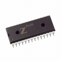
Z8F0822PJ020EG Zilog, Z8F0822PJ020EG Datasheet - Page 173

Z8F0822PJ020EG
Manufacturer Part Number
Z8F0822PJ020EG
Description
IC ENCORE MCU FLASH 8K 28DIP
Manufacturer
Zilog
Series
Encore!® XP®r
Datasheet
1.Z8F08200100KIT.pdf
(264 pages)
Specifications of Z8F0822PJ020EG
Core Processor
Z8
Core Size
8-Bit
Speed
20MHz
Connectivity
I²C, IrDA, SPI, UART/USART
Peripherals
Brown-out Detect/Reset, POR, PWM, WDT
Number Of I /o
19
Program Memory Size
8KB (8K x 8)
Program Memory Type
FLASH
Ram Size
1K x 8
Voltage - Supply (vcc/vdd)
2.7 V ~ 3.6 V
Data Converters
A/D 5x10b
Oscillator Type
Internal
Operating Temperature
-40°C ~ 105°C
Package / Case
28-DIP (0.600", 15.24mm)
Processor Series
Z8F082xx
Core
eZ8
Data Bus Width
8 bit
Data Ram Size
1 KB
Interface Type
I2C, SPI, UART
Maximum Clock Frequency
20 MHz
Number Of Programmable I/os
19
Number Of Timers
2
Operating Supply Voltage
2.7 V to 3.6 V
Maximum Operating Temperature
+ 105 C
Mounting Style
Through Hole
Minimum Operating Temperature
- 40 C
On-chip Adc
10 bit, 5 Channel
Lead Free Status / RoHS Status
Lead free / RoHS Compliant
Eeprom Size
-
Lead Free Status / Rohs Status
Details
Other names
269-4207
Z8F0822PJ020EG
Z8F0822PJ020EG
- Current page: 173 of 264
- Download datasheet (6Mb)
Table 84. Flash Status Register (FSTAT)
Table 85. Page Select Register (FPS)
PS022517-0508
BITS
FIELD
RESET
R/W
ADDR
BITS
FIELD
RESET
R/W
ADDR
Flash Status Register
Page Select Register
7
INFO_EN
7
The Flash Status Register
This register can be read at any time. The Read-only Flash Status Register shares its Reg-
ister File address with the Write-only Flash Control Register.
Reserved
These bits are reserved and must be 0.
FSTAT—Flash Controller Status
00_0000 = Flash Controller locked.
00_0001 = First unlock command received.
00_0010 = Second unlock command received.
00_0011 = Flash Controller unlocked.
00_0100 = Flash Sector Protect Register selected.
00_1xxx = Program operation in progress.
01_0xxx = Page erase operation in progress.
10_0xxx = Mass erase operation in progress.
The Page Select (FPS) Register
programmed. Each Flash Page contains 512 bytes of Flash memory. During a Page Erase
operation, all Flash memory locations with the 7 most significant bits of the address given
by the PAGE field are erased to
The Page Select Register shares its Register File address with the Flash Sector Protect
Register. The Page Select Register cannot be accessed when the Flash Sector Protect
Register is enabled.
Reserved
6
6
5
5
(Table
4
(Table
FFH
84) indicates the current state of the Flash Controller.
4
.
85) selects the Flash memory page to be erased or
FF8H
FF9H
R/W
R
0
0
3
PAGE
3
FSTAT
2
Z8 Encore! XP
2
Product Specification
1
1
®
F0822 Series
Flash Memory
0
0
160
Related parts for Z8F0822PJ020EG
Image
Part Number
Description
Manufacturer
Datasheet
Request
R

Part Number:
Description:
Communication Controllers, ZILOG INTELLIGENT PERIPHERAL CONTROLLER (ZIP)
Manufacturer:
Zilog, Inc.
Datasheet:

Part Number:
Description:
KIT DEV FOR Z8 ENCORE 16K TO 64K
Manufacturer:
Zilog
Datasheet:

Part Number:
Description:
KIT DEV Z8 ENCORE XP 28-PIN
Manufacturer:
Zilog
Datasheet:

Part Number:
Description:
DEV KIT FOR Z8 ENCORE 8K/4K
Manufacturer:
Zilog
Datasheet:

Part Number:
Description:
KIT DEV Z8 ENCORE XP 28-PIN
Manufacturer:
Zilog
Datasheet:

Part Number:
Description:
DEV KIT FOR Z8 ENCORE 4K TO 8K
Manufacturer:
Zilog
Datasheet:

Part Number:
Description:
CMOS Z8 microcontroller. ROM 16 Kbytes, RAM 256 bytes, speed 16 MHz, 32 lines I/O, 3.0V to 5.5V
Manufacturer:
Zilog, Inc.
Datasheet:

Part Number:
Description:
Low-cost microcontroller. 512 bytes ROM, 61 bytes RAM, 8 MHz
Manufacturer:
Zilog, Inc.
Datasheet:

Part Number:
Description:
Z8 4K OTP Microcontroller
Manufacturer:
Zilog, Inc.
Datasheet:

Part Number:
Description:
CMOS SUPER8 ROMLESS MCU
Manufacturer:
Zilog, Inc.
Datasheet:

Part Number:
Description:
SL1866 CMOSZ8 OTP Microcontroller
Manufacturer:
Zilog, Inc.
Datasheet:

Part Number:
Description:
SL1866 CMOSZ8 OTP Microcontroller
Manufacturer:
Zilog, Inc.
Datasheet:

Part Number:
Description:
OTP (KB) = 1, RAM = 125, Speed = 12, I/O = 14, 8-bit Timers = 2, Comm Interfaces Other Features = Por, LV Protect, Voltage = 4.5-5.5V
Manufacturer:
Zilog, Inc.
Datasheet:

Part Number:
Description:
Manufacturer:
Zilog, Inc.
Datasheet:


