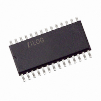
Z8673312SSG Zilog, Z8673312SSG Datasheet - Page 41

Z8673312SSG
Manufacturer Part Number
Z8673312SSG
Description
IC MICROCONTROLLER 8K 28-SOIC
Manufacturer
Zilog
Series
Z8®r
Datasheet
1.Z86E3312SSC.pdf
(84 pages)
Specifications of Z8673312SSG
Core Processor
Z8
Core Size
8-Bit
Speed
12MHz
Connectivity
EBI/EMI
Peripherals
POR, WDT
Number Of I /o
24
Program Memory Size
8KB (8K x 8)
Program Memory Type
OTP
Ram Size
237 x 8
Voltage - Supply (vcc/vdd)
3.5 V ~ 5.5 V
Oscillator Type
Internal
Operating Temperature
0°C ~ 70°C
Package / Case
28-SOIC (7.5mm Width)
Processor Series
Z8673x
Core
Z80
Data Bus Width
8 bit
Data Ram Size
237 B
Maximum Clock Frequency
12 MHz
Number Of Programmable I/os
24
Number Of Timers
2
Operating Supply Voltage
4.75 V to 5.25 V
Maximum Operating Temperature
+ 70 C
Mounting Style
SMD/SMT
Minimum Operating Temperature
0 C
Lead Free Status / RoHS Status
Lead free / RoHS Compliant
Eeprom Size
-
Data Converters
-
Lead Free Status / Rohs Status
Details
Other names
269-3940
Z8673312SSG
Z8673312SSG
Available stocks
Company
Part Number
Manufacturer
Quantity
Price
Company:
Part Number:
Z8673312SSG
Manufacturer:
Zilog
Quantity:
11
Table 18. Additional Timing Table (Divide by Two Mode) T
Pin Functions
PS022901-0508
No Symbol Parameter
12 Twdt
Notes
1. The V
2. Timing Reference uses 0.7 VC0 for a logic 1 and 0.2 VGC for a logic 0.
3. SMR D1 = 0.
4. SMR-D5 = 1, POR STOP Mode Delay is on
5. Interrupt request via Port 3 (P31-P33)
6. Interrupt request via Port 3 (P30).
7. Maximum frequency for internal system clock is 2 MHz when using Low EMI OSC PCON Bit D7 = 0
8. Reg. WDTMR.
9. Using internal RC.
guarantees only 3.5 V.
EPROM Programming Mode
CC
voltage specification of 5.5 V guarantees 5.0 V ± 0.5 V and the V
Watchdog Timer
Delay Time Before
Timeout
D7-D0 Data Bus. The data can be read from or written to external memory through the
data bus.
V
ing other modes.
CE Chip Enable (active Low). This pin is active during EPROM Read Mode, Program
Mode, and Program Verify Mode.
OE Output Enable (active Low). This pin drives the direction of the Data Bus. When this
pin is Low, the Data Bus is output, when High, the Data Bus is input.
EPM EPROM Program Mode. This pin controls the different EPROM Program Mode by
applying different voltages.
V
PGM Program Mode (active Low). When this pin is Low, the data is programmed to the
EPROM through the Data Bus.
CC
PP
Program Voltage. This pin supplies the program voltage.
Power Supply. This pin must supply 5 V during the EPROM read mode and 6 V dur-
V
3.5V
5.5V
3.5V
5.5V
3.5V
5.5V
3.5V
5.5V
CC
1
Min
7
3.5
14
7
28
14
112
56
Max
Min
10
5
20
10
40
20
160
80
A
= -40 °C to +105 °C (Continued)
Max
CMOS Z8
CC
voltage specification of 3.5 V
Units Conditions
ms
ms
ms
ms
ms
ms
ms
ms
®
Product Specification
OTP Microcontrollers
D1 = 0
D0 =1
D1 = 0
D1 = 0
D1 = 1
D0 = 1
D1 = 1
D0 =0
Electrical Characteristics
5,11
5,11
5,11
Notes
8,9
5,11
5,11
5,11
5,11
37


