Z8673312SSG Zilog, Z8673312SSG Datasheet - Page 65
Z8673312SSG
Manufacturer Part Number
Z8673312SSG
Description
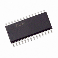
IC MICROCONTROLLER 8K 28-SOIC
Manufacturer
Zilog
Series
Z8®r
Datasheet
1.Z86E3312SSC.pdf
(84 pages)
Specifications of Z8673312SSG
Core Processor
Z8
Core Size
8-Bit
Speed
12MHz
Connectivity
EBI/EMI
Peripherals
POR, WDT
Number Of I /o
24
Program Memory Size
8KB (8K x 8)
Program Memory Type
OTP
Ram Size
237 x 8
Voltage - Supply (vcc/vdd)
3.5 V ~ 5.5 V
Oscillator Type
Internal
Operating Temperature
0°C ~ 70°C
Package / Case
28-SOIC (7.5mm Width)
Processor Series
Z8673x
Core
Z80
Data Bus Width
8 bit
Data Ram Size
237 B
Maximum Clock Frequency
12 MHz
Number Of Programmable I/os
24
Number Of Timers
2
Operating Supply Voltage
4.75 V to 5.25 V
Maximum Operating Temperature
+ 70 C
Mounting Style
SMD/SMT
Minimum Operating Temperature
0 C
Lead Free Status / RoHS Status
Lead free / RoHS Compliant
Eeprom Size
-
Data Converters
-
Lead Free Status / Rohs Status
Details
Other names
269-3940
Z8673312SSG
Z8673312SSG
Available stocks
Company
Part Number
Manufacturer
Quantity
Price
Company:

Part Number:
Z8673312SSG
Manufacturer:
Zilog
Quantity:
11


PS022901-0508
Table 22. Stop Mode Recovery Source
Stop Mode Recovery Delay Select (D5). The 5 ms RESET delay after Stop Mode Recov-
ery is disabled by programming this bit to a zero. A “1” in this bit will cause a 5 ms
RESET delay after Stop Mode Recovery. The default condition of this bit is 1. If the fast
wake up mode is selected, the Stop Mode Recovery source needs to be kept active for at
least 5TpC.
Stop Mode Recovery Level Select (D6). A “1” in this bit defines that a high level on any
one of the recovery sources wakes the MCU from STOP Mode. A 0 defines low level
recovery. The default value is 0.
Cold or Warm Start (D7). This bit is set by the device upon entering STOP Mode. A “0”
in this bit indicates that the device has been reset by POR (cold). A “1” in this bit indicates
the device was awakened by a SMR source (warm).
Stop Mode Recovery Register 2 (SMR2). This register contains additional Stop Mode
Recovery sources. When the Stop Mode Recovery sources are selected in this register then
SMR Register Bits D2, D3, and D4 must be 0.
Watchdog Timer Mode Register (WDTMR). The WDT is a retriggerable one-shot timer
that resets the Z8 if it reaches its terminal count. The WDT is disabled after Power-On
D4
0
0
0
0
1
1
1
1
D3
0
0
1
1
0
0
1
1
D1
0
0
1
SMR:10
D2
0
1
0
1
0
1
0
1
DO
0
1
0
SMR Source selection
POR recovery only
P30 transition
P31 transition (Not in analog mode)
P32 transition (Not in analog mode)
P33 transition (Not in analog mode)
P27 transition
Logical NOR of Port 2 bits 0-3
Logical NOR of Port 2 bits 0-7
POR and/or external reset recovery
Logical AND of P20 through P23
Logical AND of P20 through P27
Description of Action
Operation
CMOS Z8
®
Product Specification
OTP Microcontrollers
Electrical Characteristics
61
Related parts for Z8673312SSG
Image
Part Number
Description
Manufacturer
Datasheet
Request
R

Part Number:
Description:
Communication Controllers, ZILOG INTELLIGENT PERIPHERAL CONTROLLER (ZIP)
Manufacturer:
Zilog, Inc.
Datasheet:

Part Number:
Description:
KIT DEV FOR Z8 ENCORE 16K TO 64K
Manufacturer:
Zilog
Datasheet:

Part Number:
Description:
KIT DEV Z8 ENCORE XP 28-PIN
Manufacturer:
Zilog
Datasheet:

Part Number:
Description:
DEV KIT FOR Z8 ENCORE 8K/4K
Manufacturer:
Zilog
Datasheet:

Part Number:
Description:
KIT DEV Z8 ENCORE XP 28-PIN
Manufacturer:
Zilog
Datasheet:

Part Number:
Description:
DEV KIT FOR Z8 ENCORE 4K TO 8K
Manufacturer:
Zilog
Datasheet:
Part Number:
Description:
CMOS Z8 microcontroller. ROM 16 Kbytes, RAM 256 bytes, speed 16 MHz, 32 lines I/O, 3.0V to 5.5V
Manufacturer:
Zilog, Inc.
Datasheet:
Part Number:
Description:
Low-cost microcontroller. 512 bytes ROM, 61 bytes RAM, 8 MHz
Manufacturer:
Zilog, Inc.
Datasheet:
Part Number:
Description:
Z8 4K OTP Microcontroller
Manufacturer:
Zilog, Inc.
Datasheet:
Part Number:
Description:
CMOS SUPER8 ROMLESS MCU
Manufacturer:
Zilog, Inc.
Datasheet:
Part Number:
Description:
SL1866 CMOSZ8 OTP Microcontroller
Manufacturer:
Zilog, Inc.
Datasheet:
Part Number:
Description:
SL1866 CMOSZ8 OTP Microcontroller
Manufacturer:
Zilog, Inc.
Datasheet:
Part Number:
Description:
OTP (KB) = 1, RAM = 125, Speed = 12, I/O = 14, 8-bit Timers = 2, Comm Interfaces Other Features = Por, LV Protect, Voltage = 4.5-5.5V
Manufacturer:
Zilog, Inc.
Datasheet:
Part Number:
Description:
Manufacturer:
Zilog, Inc.
Datasheet: