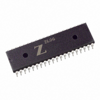
Z86E7216PSG Zilog, Z86E7216PSG Datasheet - Page 29

Z86E7216PSG
Manufacturer Part Number
Z86E7216PSG
Description
IC 16K OTP ZIRC 40-DIP
Manufacturer
Zilog
Series
Z8®r
Datasheet
1.Z86E7216PSC.pdf
(102 pages)
Specifications of Z86E7216PSG
Core Processor
Z8
Core Size
8-Bit
Speed
16MHz
Peripherals
LVD, POR, WDT
Number Of I /o
31
Program Memory Size
16KB (16K x 8)
Program Memory Type
OTP
Ram Size
748 x 8
Voltage - Supply (vcc/vdd)
3 V ~ 5.5 V
Oscillator Type
Internal
Operating Temperature
0°C ~ 70°C
Package / Case
40-DIP (0.620", 15.75mm)
Lead Free Status / RoHS Status
Lead free / RoHS Compliant
Eeprom Size
-
Data Converters
-
Connectivity
-
- Current page: 29 of 102
- Download datasheet (2Mb)
Pin Functions
PS008704-0507
/DS (Output, Active Low)
/AS (Output, Active Low)
XTAL1 Crystal 1 (Time-Based Input)
XTAL2 Crystal 2 (Time-Based Output)
R//W Read/Write (Output, Write Low)
R//RL (Input)
Port 0 (P07–P00)
Note:
Data Strobe is activated once for each external memory transfer. For a READ
operation, data must be available before the trailing edge of /DS. For WRITE
operations, the falling edge of /DS indicates that output data is valid.
Address Strobe is pulsed once at the beginning of each machine cycle. Address
output is through Port 0/Port 1 for all external programs. Memory address trans-
fers are valid at the trailing edge of /AS. Under program control, /AS is placed in
the high-impedance state along with Ports 0 and 1, Data Strobe, and Read/Write.
This pin connects a parallel-resonant crystal, ceramic resonator, LC, or RC net-
work or an external single-phase clock to the on-chip oscillator input.
This pin connects a parallel-resonant, crystal, ceramic resonant, LC, or RC net-
work to the on-chip oscillator output.
The R//W signal is Low when the CCP is writing to the external program or data
memory.
This pin, when connected to GND, disables the internal ROM and forces the
device to function as a ROMless Z8.
Port 0 is an 8-bit, bidirectional, CMOS-compatible port. These eight I/O lines are
configured under software control as a nibble I/O port or as an address port for
interfacing external memory. The output drivers are push-pull. Port 0 is placed
under handshake control. In this configuration, Port 3, lines P32 and P35 are
used as the handshake control /DAV0 and RDY0. Handshake signal direction is
When left unconnected or pulled high to V
normally as a Z8 ROM version.
CC
, the part functions
OTP Microcontroller
25
Related parts for Z86E7216PSG
Image
Part Number
Description
Manufacturer
Datasheet
Request
R

Part Number:
Description:
Otp Microcontroller
Manufacturer:
ZiLOG Semiconductor
Datasheet:

Part Number:
Description:
Communication Controllers, ZILOG INTELLIGENT PERIPHERAL CONTROLLER (ZIP)
Manufacturer:
Zilog, Inc.
Datasheet:

Part Number:
Description:
KIT DEV FOR Z8 ENCORE 16K TO 64K
Manufacturer:
Zilog
Datasheet:

Part Number:
Description:
KIT DEV Z8 ENCORE XP 28-PIN
Manufacturer:
Zilog
Datasheet:

Part Number:
Description:
DEV KIT FOR Z8 ENCORE 8K/4K
Manufacturer:
Zilog
Datasheet:

Part Number:
Description:
KIT DEV Z8 ENCORE XP 28-PIN
Manufacturer:
Zilog
Datasheet:

Part Number:
Description:
DEV KIT FOR Z8 ENCORE 4K TO 8K
Manufacturer:
Zilog
Datasheet:

Part Number:
Description:
CMOS Z8 microcontroller. ROM 16 Kbytes, RAM 256 bytes, speed 16 MHz, 32 lines I/O, 3.0V to 5.5V
Manufacturer:
Zilog, Inc.
Datasheet:

Part Number:
Description:
Low-cost microcontroller. 512 bytes ROM, 61 bytes RAM, 8 MHz
Manufacturer:
Zilog, Inc.
Datasheet:

Part Number:
Description:
Z8 4K OTP Microcontroller
Manufacturer:
Zilog, Inc.
Datasheet:

Part Number:
Description:
CMOS SUPER8 ROMLESS MCU
Manufacturer:
Zilog, Inc.
Datasheet:

Part Number:
Description:
SL1866 CMOSZ8 OTP Microcontroller
Manufacturer:
Zilog, Inc.
Datasheet:

Part Number:
Description:
SL1866 CMOSZ8 OTP Microcontroller
Manufacturer:
Zilog, Inc.
Datasheet:

Part Number:
Description:
OTP (KB) = 1, RAM = 125, Speed = 12, I/O = 14, 8-bit Timers = 2, Comm Interfaces Other Features = Por, LV Protect, Voltage = 4.5-5.5V
Manufacturer:
Zilog, Inc.
Datasheet:


