CY8CLED16P01-28PVXIT Cypress Semiconductor Corp, CY8CLED16P01-28PVXIT Datasheet
CY8CLED16P01-28PVXIT
Specifications of CY8CLED16P01-28PVXIT


Related parts for CY8CLED16P01-28PVXIT


CY8CLED16P01-28PVXIT Summary of contents
Page 1
... SPI, UART etc. PLC Core PSoC Core Powerline Transceiver Packet AC/DC Powerline Coupling Circuit (110V/240V AC, 12V/24V AC/DC etc.) Powerline • 198 Champion Court • San Jose CY8CLED16P01 TM Masters or Slaves Modulation Technology PrISM, PWM etc. Additional Communication Interface DALI, DMX512 HB LED Controller ...
Page 2
... PLC Functional Overview The CY8CLED16P01 is an integrated Powerline Communication (PLC) chip with the Powerline Modem PHY and Network Protocol Stack running on the same device. Apart from the PLC core, the CY8CLED16P01 also offers Cypress's revolutionary PSoC technology that enables system designers to integrate multiple functions on the same chip. 1.1 Robust Communication using Cypress’ ...
Page 3
... Coupling Circuit Reference Design The coupling circuit couples low voltage signals from the CY8CLED16P01 to the powerline. The topology of this circuit is determined by the voltage on the powerline and design constraints mandated by powerline usage regulations. Cypress provides reference designs for a range of powerline voltages including 110V/240V AC and 12V/24V AC/DC. The ...
Page 4
... Group addressing: This is explained in the next section. ■ 1.3.8 Group Membership Group membership enables the user to multicast messages to describes the select groups. The CY8CLED16P01 supports two types of group addressing: Single Group Membership – The network protocol supports up ■ to 256 different groups on the network in this mode. In this Description mode, each PLC node can only be part of a single group ...
Page 5
... Transmit response data to a Payload = Local TX Remote Node. Data Enables/Disables BIU function Enable Remote BIU ality at the remote node 1 - Disable Remote BIU CY8CLED16P01 Response (RX Data) If Remote Lock Config = 0, Response = 00 (Success) If Remote Lock Config = 1, Response = 01 (Denied) If Remote Lock Config = 0, Response = 00 (Success) If Remote Lock Config = 1, ...
Page 6
... Byte0 - Remote SIngle the Remote node Group Membership Address Byte1- Remote Multiple Group Membership Address None the Remote node CY8CLED16P01 Response (RX Data) If Remote Lock Config = 0, Response = 00 (Success) If Remote Lock Config = 1, Response = 01 (Denied) If Remote Lock Config = 0, Response = 00 (Success) If Remote Lock Config = 1, Response = 01 (Denied) ...
Page 7
... PWM. LED dimming modulators use digital block resources. Digital blocks are configurable 8-bit digital peripherals. There are two types of digital blocks in the CY8CLED16P01: basic and commu- nication. Usually, there are equal numbers of each. Any commu- nication functions must be implemented using communication blocks but basic, noncommunication functions are implemented using either kind of block ...
Page 8
... LED Temperature Compensation Many HB LED systems need to measure analog signals. One or more thermistors are often present to measure temperatures of the system and the LEDs. The CY8CLED16P01 measures an analog signal with an analog-to-digital converter (ADC). The device can implement a variety of flexible ADC implementations. ...
Page 9
... For instance, consider the application to remotely control LED color/intensity (with current feedback) over powerlines using the CY8CLED16P01 for both PLC and LED color control. The PLC Communication functionality and the current feedback do not necessarily need to Digital Blocks happen at the same time ...
Page 10
... System Resources. Configurable global busing enables all the device resources to be combined into a complete custom system. The CY8CLED16P01 family can have up to five I/O ports that connect to the global digital and analog interconnects, providing access to 16 digital blocks and 12 analog blocks. ...
Page 11
... Figure 3-3. Digital System Block Diagram Port 7 Port 6 Modulation Technology PrISM, PWM etc. Additional Communication Interface DALI, DMX512 HB LED Controller 8 8 GIE[7:0] GIO[7:0] CY8CLED16P01 Port 5 Port 3 Port 1 Port 4 Port 2 Port 0 To System Bus To Analog System DIGITAL SYSTEM Digital PSoC Block Array Row 0 4 DBB00 DBB01 ...
Page 12
... Many other topologies possible ■ Analog blocks are provided in columns of three, which includes one CT (continuous time) and two SC (switched capacitor) blocks, as shown in the Figure 3-4. on page 12. Document Number: 001-49263 Rev. *E CY8CLED16P01 Figure 3-4. Analog System Block Diagram P0[7] P0[5] P0[3] P0[1] P2[3] P2[1] ...
Page 13
... PSoC Designer can be downloaded from www.cypress.com/PSoCDesigner. PSoC Designer 5.0 SP5 or later provides support for CY8CLED16P01 devices. This data Modulation sheet is an overview of the CY8CLED16P01 integrated circuit Technology and presents specific pin, register, and electrical specifications. PrISM, PWM etc. For in depth information, along with detailed programming ...
Page 14
... USB port. The base unit is universal and operates with all PSoC devices. Emulation pods for each device family are available separately. The emulation pod takes the place of the PSoC device in the target board and performs full speed (24 MHz) operation. CY8CLED16P01 Page [+] Feedback [+] Feedback ...
Page 15
... Designer. These data sheets explain the internal operation of the component and provide performance specifications. Each data sheet describes the use of each user module parameter or driver Document Number: 001-49263 Rev. *E CY8CLED16P01 property, and other information you may need to successfully implement your design. 6.3 Organize and Connect ...
Page 16
... CY8CLED16P01 chip with the PLT User Module, loaded along with the other User Modules. 6.1 Intelligent Lighting User Modules The CY8CLED16P01 has the intelligent lighting control user modules along with the PLC user modules. These user modules enable the user to do the following: Document Number: 001-49263 Rev ...
Page 17
... ROM read only memory SC switched capacitor SRAM static random access memory Document Number: 001-49263 Rev. *E CY8CLED16P01 7.2 Units of Measure A units of measure table is located in the section Specifications on page 25. 7.3 Numeric Naming Hexadecimal numbers are represented with all letters in uppercase with an appended lowercase ‘h’ (for example, ‘14h’ or ‘ ...
Page 18
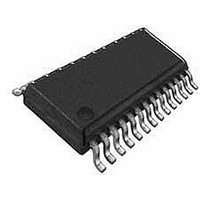
... Pin Information The CY8CLED16P01 PLC device is available in a variety of packages which are listed and illustrated in the following tables. Every port pin (labeled with a “P”) is capable of Digital I/O. However, Vss, Vdd, and XRES are not capable of Digital I/O. 8.1 28-Pin Part Pinout Table 8-1 ...
Page 19
... Logic ‘1’ - When the Modem is not trans- mitting 48 IO P2[5] LEGEND Analog Input Output, and RSVD = Reserved (should be left unconnected). Note 3. The QFN package has a center pad that must be connected to ground (Vss). Document Number: 001-49263 Rev. *E Figure 8-2. CY8CLED16P01 48-Pin PLC Device Description P2[ P2[1] 2 P4[7] 3 P4[5] ...
Page 20
... Part Pinout (On-Chip Debug) The 100-pin TQFP part is for the CY8CLED16P01-OCD On-Chip Debug PLC device. Note that the OCD parts are only used for in-circuit debugging. OCD parts are not available for production. Table 8-3. 100-Pin OCD Part Pinout (TQFP) ...
Page 21
... OCDE 12 OCDO 13 RSVD 14 Vss 15 P3[7] 16 P3[5] 17 P3[3] 18 P3[1] 19 P5[7] 20 P5[5] 21 P5[3] 22 P5[ SCL, P1[ Document Number: 001-49263 Rev. *E Figure 8-3. CY8CLED16P01-OCD OCD TQFP Not for Production CY8CLED16P01 RSVD P2[6] , External VREF AGND 69 RXCOMP _IN RXCOMP _ OUT 68 67 P4[6] P4[4] 66 Vss 65 P4[ P4[0] ...
Page 22
... Register Reference This section lists the registers of the CY8CLED16P01 PLC device. For detailed register information, refer to the PLC Technical Reference Manual . 9.1 Register Conventions The register conventions specific to this section are listed in the following table. Convention Description R Read register or bit(s) W Write register or bit(s) ...
Page 23
... ASD20CR1 ASD20CR2 92 53 ASD20CR3 ASC21CR0 ASC21CR1 ASC21CR2 96 57 ASC21CR3 ASD22CR0 ASD22CR1 ASD22CR2 9A 5B ASD22CR3 ASC23CR0 ASC23CR1 ASC23CR2 9E 5F ASC23CR3 Access is bit specific. CY8CLED16P01 Access Name Addr Access (0,Hex) R MUL0_DH MUL0_DL ACC0_DR1 ACC0_DR0 ACC0_DR3 ACC0_DR2 CPU_F CPU_SCR1 FE # CPU_SCR0 FF # Addr Access Name Access ...
Page 24
... RDI0RI RDI0SYN RDI0IS RDI0LT0 RDI0LT1 RDI0RO0 RDI0RO1 RDI1RI RDI1SYN RDI1IS RDI1LT0 RDI1LT1 RDI1RO0 RDI1RO1 Access is bit specific. CY8CLED16P01 Addr Access Name Access (1,Hex DEC_CR2 E7 RW IMO_TR E8 W ILO_TR E9 W BDG_TR EA RW ECO_TR CPU_F FLS_PR1 CPU_SCR1 FE # CPU_SCR0 FF # Page [+] Feedback [+] Feedback ...
Page 25
... Electrical Specifications This section presents the DC and AC electrical specifications of the CY8CLED16P01 device. For the most up to date electrical spec- ifications, confirm that you have the most recent data sheet by going to the web at Specifications are valid for -40°C ≤ T ≤ 85°C and T A The following table lists the units of measure that are used in this section ...
Page 26
... V 2.1 – V – 60 – mV Gross tested to 1 μ A. – 1 – nA – 3 Package and pin dependent. Temp = 25°C. – 3 Package and pin dependent. Temp = 25°C. CY8CLED16P01 Notes Thermal on page 41.The user must limit Notes = 25°C, A Notes Page [+] Feedback [+] Feedback ...
Page 27
... A – 2400 3200 μ A – 4600 6400 Vss ≤ VIN ≤ (Vdd - 2.25 – dB (Vdd - 1.25V) ≤ VIN ≤ Vdd . Min Typ Max Units 0.2 – Vdd - 1 V μ A – – 2 CY8CLED16P01 Notes Notes Page [+] Feedback [+] Feedback ...
Page 28
... Vdd - – – 0.5 × Vdd - – 1.1 – 2 Min 1.28 Vdd/2 - 0.02 2.52 [4] P2[4] - 0.013 1.27 2.03 [4] -0.034 Vdd/2 + 1.21 3.75 P2[6] + 2.478 P2[4] + 1.218 CY8CLED16P01 Max Units Notes 12 mV μ V/°C – Vdd - 1 – V – 1 – ...
Page 29
... Units k Ω – 12.2 – – 80 – fF Min Typ Max Units – 4.55 – V – 4.55 – V – 0 – mV 4.63 4.73 4.82 V 4.72 4.81 4.91 V CY8CLED16P01 Max Units 2. 0.129 V V P2[ 0.107 V P2[4] - P2[6] + 0.110 V Notes Notes Page [+] Feedback [+] Feedback ...
Page 30
... Typ Max 23.4 24 24.6 [6] 5.5 6 6.5 0.93 24 24 – 32.768 – http://www.cypress.com CY8CLED16P01 Units Notes Driving internal pull down resistor mA Driving internal pull down resistor V V – Erase/write cycles per block – Erase/write cycles Years Units Notes MHz Trimmed for 5V operation using factory trim values ...
Page 31
... Figure 10-1. PLL Lock Timing Diagram T PLLSLEW CY8CLED16P01 Units Notes – kHz After a reset and before the m8c starts to run, the ILO is not trimmed. See the System Resets section of the PSoC Technical Reference Manual for details on timing this. ...
Page 32
... TFallS Fall Time, Slow Strong Mode, Cload = 50 pF Document Number: 001-49263 Rev MHz PLLSLEWLOW T OS Jitter24M1 Jitter32k Min Typ Max Units 0 – 12.3 MHz 3 – – – – ns CY8CLED16P01 32 kHz Notes Normal Strong Mode 10% - 90% 10% - 90% 10% - 90% 10% - 90% Page [+] Feedback [+] Feedback ...
Page 33
... CY8CLED16P01 Units Notes μ s μ s μ s μ s μ s μ μ μ μ μ μ μ s MHz MHz MHz Page [+] Feedback [+] Feedback ...
Page 34
... LPC response time RLPC Document Number: 001-49263 Rev. *E 0.1 Freq (kHz Figure 10-8. Typical Opamp Noise 0.1 1 Freq (kHz) Min Typ Max Units – – 50 CY8CLED16P01 0 0.01 0.1 1.0 10 100 PH_BH PH_BL PM_BL PL_BL 10 100 Notes μ s ≥ overdrive comparator reference set within V . ...
Page 35
... Vdd ≥ 4.75V, 2 Stop Bits Receiver Maximum Input Clock Frequency Vdd ≥ 4.75V, 2 Stop Bits Note minimum input pulse width is based on the input synchronizers running at 24 MHz (42 ns nominal period Document Number: 001-49263 Rev. *E CY8CLED16P01 Min Typ Max Units 49.2 MHz ...
Page 36
... Min Typ Max 1 – – – – 40 – – 0 – 8 – 10 – – 40 – CY8CLED16P01 Units Notes μ μ μ s 3.4 μ s 3.4 V/ μ s – V/ μ s – V/ μ s – V/ μ s – – MHz – MHz – kHz – kHz ...
Page 37
... T SUDATI2C HDSTAI2C T Sr SUSTAI2C at http://www.cypress.com for more information. CY8CLED16P01 Max Units Notes 45 ns – ms Erase all Blocks and protection fields at once [9] 100 ms 0°C <= Tj <= 100°C [9] 200 ms -40°C <= Tj <= 0°C ...
Page 38
... Packaging Information This section illustrates the packaging specifications for the CY8CLED16P01 PLC device, along with the thermal impedances for each package, and the typical package capacitance on crystal pins. Note Emulation tools may require a larger area on the target PCB than the chip’s footprint. For a detailed description of the emulation tools’ ...
Page 39
... Important Note For information on the preferred dimensions for mounting QFN packages, see the following Application Note at http://www.amkor.com/products/notes_papers/MLFAppNote.pdf. Important Note Pinned vias for thermal conduction are not required for the low-power PSoC devices. Document Number: 001-49263 Rev. *E Figure 11-2. 48-Pin (7x7 mm) QFN CY8CLED16P01 001-12919 *A Page [+] Feedback [+] Feedback ...
Page 40
... Figure 11-3. 48-Pin QFN 7x7x 0.90 MM (Sawn Type) Document Number: 001-49263 Rev. *E Figure 11-4. 100-Pin TQFP CY8CLED16P01 001-13191 *D 51-85048 51-85048 ** ** 51-85048 *C Page [+] Feedback [+] Feedback ...
Page 41
... Refer to the solder manufacturer specifications. Document Number: 001-49263 Rev. *E [11] JA 94°C/W 28°C/W 50°C/W 2.8 pF 1.8 pF 3.1 pF [13] Minimum Peak Temperature 240°C 220°C 220°C CY8CLED16P01 Maximum Peak Temperature 260°C 260°C 260°C Page [+] Feedback [+] Feedback ...
Page 42
... CY3276 - Programmable HV PLC + EZ-Color™ Devel- opment Kit The CY3276 is used for prototyping and development on the CY8CLED16P01 with PSoC Designer. This kit supports in-circuit emulation. The software interface enables users to run, halt, and single-step the processor and view the content of specific memory locations ...
Page 43
... Getting Started Guide ■ Wire Pack ■ Document Number: 001-49263 Rev. *E CY8CLED16P01 12.4 Device Programmers All device programmers are purchased from the Cypress Online Store. 12.4.1 CY3216 Modular Programmer The CY3216 Modular Programmer kit features a modular programmer and the MiniProg1 programming unit. The modular programmer includes three programming module cards and supports multiple Cypress products ...
Page 44
... The following table lists the CY8CLED16P01 PLC device family key package features and ordering codes. Table 13-1. CY8CLED16P01 PLC Device Key Features and Ordering Information 28-Pin (210 Mil) SSOP CY8CLED16P01-28PVXI 28-Pin (210 Mil) SSOP CY8CLED16P01-28PVXIT (Tape and Reel) 48-Pin QFN CY8CLED16P01-48LFXI 48-Pin QFN (Sawn) ...
Page 45
... Modified FIMO6, TWRITE, and Power Up IMO to Switch specifications - Added IOH, IOL, DCILO, F32K_U, TPOWERUP, TERASEALL, and SRPOWER_UP specifications Added 48-Pin QFN (Sawn) package diagram and CY8CLED16P01-48LTXI and CY8CLED16P01-48LTXIT part details in the Ordering Information table Updated section 5 and Tables 10-1, 10-2, and 10-3 to state the requirement to ...
Page 46
... PSoC® and CapSense® are registered trademarks and PSoC Designer and EZ-Color are trademarks of Cypress Semiconductor Corp. All products and company names mentioned in this document may be the trademarks of their respective holders. psoc.cypress.com clocks.cypress.com image.cypress.com Revised October 05, 2009 CY8CLED16P01 Page [+] Feedback [+] Feedback ...