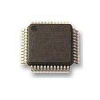
MC9S08MP16VLF Freescale Semiconductor, MC9S08MP16VLF Datasheet - Page 27

MC9S08MP16VLF
Manufacturer Part Number
MC9S08MP16VLF
Description
MCU 8BIT .25U SGF FLASH 48-LQFP
Manufacturer
Freescale Semiconductor
Series
HCS08r
Datasheet
1.MC9S08MP12VWL.pdf
(36 pages)
Specifications of MC9S08MP16VLF
Core Processor
HCS08
Core Size
8-Bit
Speed
51.34MHz
Connectivity
I²C, LIN, SCI, SPI
Peripherals
LVD, POR, PWM, WDT
Number Of I /o
40
Program Memory Size
16KB (16K x 8)
Program Memory Type
FLASH
Ram Size
1K x 8
Voltage - Supply (vcc/vdd)
2.7 V ~ 5.5 V
Data Converters
A/D 13x12b, D/A 3x5b
Oscillator Type
Internal
Operating Temperature
-40°C ~ 105°C
Package / Case
48-LQFP
Processor Series
S08MP
Core
HCS08
Data Bus Width
8 bit
Data Ram Size
1 KB
Interface Type
SCI
Maximum Clock Frequency
51.34 MHz
Number Of Programmable I/os
40
Number Of Timers
2
Operating Supply Voltage
- 0.3 V to + 5.8 V
Maximum Operating Temperature
+ 105 C
Mounting Style
SMD/SMT
3rd Party Development Tools
EWS08
Development Tools By Supplier
DEMO9S08MP16
Minimum Operating Temperature
- 40 C
On-chip Adc
12 bit, 13 Channel
On-chip Dac
3 DAC, 5 bit
Lead Free Status / RoHS Status
Lead free / RoHS Compliant
Eeprom Size
-
Lead Free Status / Rohs Status
Lead free / RoHS Compliant
Available stocks
Company
Part Number
Manufacturer
Quantity
Price
Company:
Part Number:
MC9S08MP16VLF
Manufacturer:
Freescale Semiconductor
Quantity:
10 000
1
2
3
Num
7a
7b
LSB in 12-bit resolution
8 MHz is required for PGA achieving 1 μs sampling time.
ADC in 12-bit mode, long sampling time, f
4
5
6
8
9
C
D
D
D
D
D
T
T
Num
2.14
This section describes timing characteristics for each peripheral system.
2.14.1
Freescale Semiconductor
1
2
3
4
5
6
Differential input voltage
Linearity (@ voltage gain)
Max gain error
PGA clock
PGA sampling frequency
Input signal bandwidth
Charge pump clock frequency
• 1x
• 2x
• 4x
• 8x
• 16x
• 32x
• normal mode (LP=0)
• low power mode (LP=1)
C
D
P
D
D
D
D
AC Characteristics
Bus frequency
(t
Internal low power oscillator period
External reset pulse width
Reset low drive
BKGD/MS setup time after issuing background debug force
reset to enter user or BDM modes
BKGD/MS hold time after issuing background debug force
reset to enter user or BDM modes
cyc
Control Timing
Parameter
= 1/f
Table 15. Programmable Gain Amplifier Electrical Specifications (continued)
Bus
)
3
1
ADC
2
= f
Rating
PGA
V
MC9S08MP16 Series Data Sheet, Rev. 1
Symbol
f
DIFFMAX
SAMPL
f
f
BW
cpclk
PGA
E
L
3
V
G
Table 16. Control Timing
–
(
1 – 1/2 LSB
2 – 1/2 LSB
16 – 4 LSB
32 – 4 LSB
4 – 1 LSB
8 – 1 LSB
V
----------------------------- -
2 Gain
DDA
–40 to 105 °C
–40 to 125 °C
×
Min
100
—
—
—
—
0
–
1.4
)
----------------------------------------------------------------------------------------------------
⎛
⎝
12
------------------------------------------------------------------
+
Symbol
18
t
t
t
MSSU
t
t
f
f
extrst
rstdrv
MSH
LPO
Bus
Bus
×
NUM_CLK_GS
f
PGA
f
SAMPL
f
Typical
PGA
16
32
34 x t
8
0
1
2
4
8
1
4
1
2
÷ 4
Min
700
100
500
100
DC
DC
÷ 8
⎞
⎠
cyc
+
-------------
f
ADC
43
Electrical Characteristics
+
Typ
------------ -
f
—
—
—
—
—
—
—
BUS
5
1
1 + 1/2 LSB
2 + 1/2 LSB
V
----------------------------- -
16 + 4 LSB
32 + 4 LSB
f
4 + 1 LSB
8 + 1 LSB
2
SAMPL
DDA
25.67
1300
Max
×
Max
20
—
—
—
—
Gain
8
—
—
2
4
–
2
1.4
÷ 2
Unit
MHz
MHz
μs
ns
ns
ns
μs
27
per second
Samples
Unit
MHz
V/V
Hz
Hz
%
V


