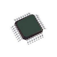
MC9S08JM8CLC Freescale Semiconductor, MC9S08JM8CLC Datasheet - Page 70

MC9S08JM8CLC
Manufacturer Part Number
MC9S08JM8CLC
Description
MCU 8BIT 8K FLASH 32-LQFP
Manufacturer
Freescale Semiconductor
Series
HCS08r
Datasheet
1.DEMO9S08JM16.pdf
(386 pages)
Specifications of MC9S08JM8CLC
Core Processor
HCS08
Core Size
8-Bit
Speed
48MHz
Connectivity
I²C, LIN, SCI, SPI, USB
Peripherals
LVD, POR, PWM, WDT
Number Of I /o
21
Program Memory Size
8KB (8K x 8)
Program Memory Type
FLASH
Ram Size
1K x 8
Voltage - Supply (vcc/vdd)
2.7 V ~ 5.5 V
Data Converters
A/D 4x12b
Oscillator Type
External
Operating Temperature
-40°C ~ 85°C
Package / Case
32-LQFP
Processor Series
S08JM
Core
HCS08
Data Bus Width
8 bit
Data Ram Size
1 KB
Interface Type
I2C, SPI
Maximum Clock Frequency
48 MHz
Number Of Programmable I/os
37
Number Of Timers
2
Operating Supply Voltage
2.7 V to 5.5 V
Maximum Operating Temperature
+ 85 C
Mounting Style
SMD/SMT
3rd Party Development Tools
EWS08
Development Tools By Supplier
DEMOJM, DEMOJMSKT, DEMOFLEXISJMSD, DEMO9S08JM16
Minimum Operating Temperature
- 40 C
On-chip Adc
12 bit, 4 Channel
Controller Family/series
HCS08
No. Of I/o's
21
Ram Memory Size
1KB
Cpu Speed
48MHz
No. Of Timers
2
Digital Ic Case Style
LQFP
Rohs Compliant
Yes
Lead Free Status / RoHS Status
Lead free / RoHS Compliant
Eeprom Size
-
Lead Free Status / Rohs Status
Lead free / RoHS Compliant
- Current page: 70 of 386
- Download datasheet (8Mb)
1
Chapter 5 Resets, Interrupts, and System Configuration
5.7.3
This register contains a single write-only control bit. A serial background command such as
WRITE_BYTE must be used to write to SBDFR. Attempts to write this register from a user program are
ignored. Reads always return 0x00.
70
Any of these reset sources that are active at the time of reset will cause the corresponding bit(s) to be set; bits corresponding
to sources that are not active at the time of reset will be cleared.
reset:
other
POR
LVR:
Field
ILOP
POR
COP
LOC
LVD
Any
PIN
7
6
5
4
2
1
W
R
U = Unaffected by reset
POR
System Background Debug Force Reset Register (SBDFR)
Power-On Reset — Reset was caused by the power-on detection logic. Because the internal supply voltage was
ramping up at the time, the low-voltage reset (LVR) status bit is also set to indicate that the reset occurred while
the internal supply was below the LVR threshold.
0 Reset not caused by POR.
1 POR caused reset.
External Reset Pin — Reset was caused by an active-low level on the external reset pin.
0 Reset not caused by external reset pin.
1 Reset came from external reset pin.
Computer Operating Properly (COP) Watchdog — Reset was caused by the COP watchdog timer timing out.
This reset source may be blocked by COPE = 0.
0 Reset not caused by COP timeout.
1 Reset caused by COP timeout.
Illegal Opcode — Reset was caused by an attempt to execute an unimplemented or illegal opcode. The STOP
instruction is considered illegal if stop is disabled by STOPE = 0 in the SOPT register. The BGND instruction is
considered illegal if active background mode is disabled by ENBDM = 0 in the BDCSC register.
0 Reset not caused by an illegal opcode.
1 Reset caused by an illegal opcode.
Loss-of-Clock Reset — Reset was caused by a loss of external clock.
0 Reset not caused by a loss of external clock.
1 Reset caused by a loss of external clock.
Low Voltage Detect — If the LVDRE and LVDSE bits are set and the supply drops below the LVD trip voltage,
an LVD reset will occur. This bit is also set by POR.
0 Reset not caused by LVD trip or POR.
1 Reset caused by LVD trip or POR.
U
1
0
7
PIN
(1)
0
0
6
Writing any value to SRS address clears COP watchdog timer.
Table 5-3. SRS Register Field Descriptions
Figure 5-3. System Reset Status (SRS)
MC9S08JM16 Series Data Sheet, Rev. 2
COP
(1)
0
0
5
ILOP
(1)
0
0
4
Description
3
0
0
0
0
LOC
(1)
0
0
2
Freescale Semiconductor
LVD
1
1
0
1
—
0
0
0
0
Related parts for MC9S08JM8CLC
Image
Part Number
Description
Manufacturer
Datasheet
Request
R
Part Number:
Description:
Manufacturer:
Freescale Semiconductor, Inc
Datasheet:
Part Number:
Description:
Manufacturer:
Freescale Semiconductor, Inc
Datasheet:
Part Number:
Description:
Manufacturer:
Freescale Semiconductor, Inc
Datasheet:
Part Number:
Description:
Manufacturer:
Freescale Semiconductor, Inc
Datasheet:
Part Number:
Description:
Manufacturer:
Freescale Semiconductor, Inc
Datasheet:
Part Number:
Description:
Manufacturer:
Freescale Semiconductor, Inc
Datasheet:
Part Number:
Description:
Manufacturer:
Freescale Semiconductor, Inc
Datasheet:
Part Number:
Description:
Manufacturer:
Freescale Semiconductor, Inc
Datasheet:
Part Number:
Description:
Manufacturer:
Freescale Semiconductor, Inc
Datasheet:
Part Number:
Description:
Manufacturer:
Freescale Semiconductor, Inc
Datasheet:
Part Number:
Description:
Manufacturer:
Freescale Semiconductor, Inc
Datasheet:
Part Number:
Description:
Manufacturer:
Freescale Semiconductor, Inc
Datasheet:
Part Number:
Description:
Manufacturer:
Freescale Semiconductor, Inc
Datasheet:
Part Number:
Description:
Manufacturer:
Freescale Semiconductor, Inc
Datasheet:
Part Number:
Description:
Manufacturer:
Freescale Semiconductor, Inc
Datasheet:


