MC9S08LL8CLF Freescale Semiconductor, MC9S08LL8CLF Datasheet - Page 10
MC9S08LL8CLF
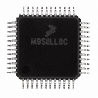
Manufacturer Part Number
MC9S08LL8CLF
Description
IC MCU 8BIT 8K FLASH 48-LQFP
Manufacturer
Freescale Semiconductor
Series
HCS08r
Datasheet
1.DEMO9S08LL16.pdf
(44 pages)
Specifications of MC9S08LL8CLF
Core Processor
HCS08
Core Size
8-Bit
Speed
20MHz
Connectivity
I²C, SCI, SPI
Peripherals
LCD, LVD, POR, PWM, WDT
Number Of I /o
31
Program Memory Size
10KB (10K x 8)
Program Memory Type
FLASH
Ram Size
2K x 8
Voltage - Supply (vcc/vdd)
1.8 V ~ 3.6 V
Data Converters
A/D 8x12b
Oscillator Type
Internal
Operating Temperature
-40°C ~ 85°C
Package / Case
48-LQFP
Processor Series
S08LL
Core
HCS08
Data Bus Width
8 bit
Data Ram Size
2 KB
Interface Type
I2C, SCI, SPI
Maximum Clock Frequency
20 MHz
Number Of Programmable I/os
31
Number Of Timers
2
Operating Supply Voltage
1.8 V to 3.6 V
Maximum Operating Temperature
+ 85 C
Mounting Style
SMD/SMT
3rd Party Development Tools
EWS08
Development Tools By Supplier
TWR-SER, TWR-ELEV, TWR-S08LL64, TWR-SENSOR-PAK, TWR-S08LL64-KIT, TWR-LCD
Minimum Operating Temperature
- 40 C
On-chip Adc
12 bit, 8 Channel
Controller Family/series
HCS08
No. Of I/o's
31
Ram Memory Size
2KB
Cpu Speed
20MHz
No. Of Timers
2
Embedded Interface Type
I2C, SCI, SPI
Rohs Compliant
Yes
Lead Free Status / RoHS Status
Lead free / RoHS Compliant
Eeprom Size
-
Lead Free Status / Rohs Status
Lead free / RoHS Compliant
Available stocks
Company
Part Number
Manufacturer
Quantity
Price
Company:

Part Number:
MC9S08LL8CLF
Manufacturer:
Freescale Semiconductor
Quantity:
10 000


Electrical Characteristics
3.3
Absolute maximum ratings are stress ratings only, and functional operation at the maxima is not
guaranteed. Stress beyond the limits specified in
damage to the device. For functional operating conditions, refer to the remaining tables in this section.
This device contains circuitry protecting against damage due to high static voltage or electrical fields;
however, it is advised that normal precautions be taken to avoid application of any voltages higher than
maximum-rated voltages to this high-impedance circuit. Reliability of operation is enhanced if unused
inputs are tied to an appropriate logic voltage level (for instance, either V
pull-up resistor associated with the pin is enabled.
10
C
D
P
T
Absolute Maximum Ratings
1
2
3
Those parameters are guaranteed during production testing on each individual device.
Those parameters are achieved by the design characterization by measuring a statistically relevant
sample size across process variations.
Those parameters are achieved by design characterization on a small sample size from typical devices
under typical conditions unless otherwise noted. All values shown in the typical column are within this
category.
Those parameters are derived mainly from simulations.
Supply voltage
Maximum current into V
Digital input voltage
Instantaneous maximum current
Storage temperature range
current-limiting resistor, calculate resistance values for positive (V
voltages, then use the larger of the two resistance values.
All functional non-supply pins, except for PTB2 are internally clamped to V
Power supply must maintain regulation within operating V
operating maximum current conditions. If positive injection current (V
I
out of regulation. Ensure external V
current. This will be the greatest risk when the MCU is not consuming power. Examples are: if
no system clock is present, or if the clock rate is very low (which would reduce overall power
consumption).
The classification is shown in the column labeled “C” in the parameter
tables where appropriate.
Input must be current limited to the value specified. To determine the value of the required
DD
Single pin limit (applies to all port pins)
, the injection current may flow out of V
Rating
MC9S08LL16 Series MCU Data Sheet, Rev. 6
DD
Table 4. Absolute Maximum Ratings
Table 3. Parameter Classifications
DD
load will shunt current greater than maximum injection
1, 2, 3
Table 4
NOTE
DD
and could result in external power supply going
may affect device reliability or cause permanent
Symbol
V
T
I
V
DD
I
DD
stg
D
In
DD
range during instantaneous and
DD
–0.3 to V
) and negative (V
In
–0.3 to 3.8
–55 to 150
SS
> V
Value
25
120
or V
SS
DD
DD
) is greater than
and V
+ 0.3
DD
) or the programmable
DD
Freescale Semiconductor
SS
.
) clamp
Unit
mA
mA
C
V
V
Related parts for MC9S08LL8CLF
Image
Part Number
Description
Manufacturer
Datasheet
Request
R

Part Number:
Description:
Manufacturer:
Freescale Semiconductor, Inc
Datasheet:
Part Number:
Description:
Manufacturer:
Freescale Semiconductor, Inc
Datasheet:
Part Number:
Description:
Manufacturer:
Freescale Semiconductor, Inc
Datasheet:
Part Number:
Description:
Manufacturer:
Freescale Semiconductor, Inc
Datasheet:
Part Number:
Description:
Manufacturer:
Freescale Semiconductor, Inc
Datasheet:
Part Number:
Description:
Manufacturer:
Freescale Semiconductor, Inc
Datasheet:
Part Number:
Description:
Manufacturer:
Freescale Semiconductor, Inc
Datasheet:
Part Number:
Description:
Manufacturer:
Freescale Semiconductor, Inc
Datasheet:
Part Number:
Description:
Manufacturer:
Freescale Semiconductor, Inc
Datasheet:
Part Number:
Description:
Manufacturer:
Freescale Semiconductor, Inc
Datasheet:
Part Number:
Description:
Manufacturer:
Freescale Semiconductor, Inc
Datasheet:
Part Number:
Description:
Manufacturer:
Freescale Semiconductor, Inc
Datasheet:
Part Number:
Description:
Manufacturer:
Freescale Semiconductor, Inc
Datasheet:
Part Number:
Description:
Manufacturer:
Freescale Semiconductor, Inc
Datasheet:
Part Number:
Description:
Manufacturer:
Freescale Semiconductor, Inc
Datasheet: