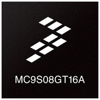
MC9S08GT16ACFCE Freescale Semiconductor, MC9S08GT16ACFCE Datasheet - Page 78

MC9S08GT16ACFCE
Manufacturer Part Number
MC9S08GT16ACFCE
Description
IC MCU 16K FLASH 2K RAM 32-QFN
Manufacturer
Freescale Semiconductor
Series
HCS08r
Datasheet
1.MC9S08GT8ACFBER.pdf
(300 pages)
Specifications of MC9S08GT16ACFCE
Core Processor
HCS08
Core Size
8-Bit
Speed
40MHz
Connectivity
I²C, SCI, SPI
Peripherals
LVD, POR, PWM, WDT
Number Of I /o
24
Program Memory Size
16KB (16K x 8)
Program Memory Type
FLASH
Ram Size
2K x 8
Voltage - Supply (vcc/vdd)
1.8 V ~ 3.6 V
Data Converters
A/D 4x10b
Oscillator Type
Internal
Operating Temperature
-40°C ~ 85°C
Package / Case
32-QFN
Processor Series
S08GT
Core
HCS08
Data Bus Width
8 bit
Data Ram Size
2 KB
Interface Type
I2C, IRSCI, SPI
Maximum Clock Frequency
20 MHz
Number Of Programmable I/os
24
Operating Supply Voltage
3.6 V
Maximum Operating Temperature
+ 85 C
Mounting Style
SMD/SMT
3rd Party Development Tools
EWS08
Development Tools By Supplier
M68EVB908GB60E, M68DEMO908GB60E
Minimum Operating Temperature
- 40 C
On-chip Adc
10 bit
For Use With
M68DEMO908GB60E - BOARD DEMO MC9S08GB60M68EVB908GB60E - BOARD EVAL FOR MC9S08GB60
Lead Free Status / RoHS Status
Lead free / RoHS Compliant
Eeprom Size
-
Lead Free Status / Rohs Status
Lead free / RoHS Compliant
- Current page: 78 of 300
- Download datasheet (2Mb)
1
LVWF will be set in the case when V
LVD reset:
Any other
Power-on
Resets, Interrupts, and System Configuration
5.7.8
This register is used to report the status of the low voltage warning function, and to configure the stop mode
behavior of the MCU.
78
LVWACK
PPDACK
reset:
reset:
LVWF
LVWV
PPDF
PPDC
LVDV
Field
PDC
W
7
6
5
4
3
2
1
0
R
Note
Note
Note
LVWF
System Power Management Status and Control 2 Register (SPMSC2)
Figure 5-10. System Power Management Status and Control 2 Register (SPMSC2)
Low-Voltage Warning Flag — The LVWF bit indicates the low voltage warning status.
0 Low voltage warning not present.
1 Low voltage warning is present or was present.
Low-Voltage Warning Acknowledge — The LVWACK bit is the low-voltage warning acknowledge. Writing a 1
to LVWACK clears LVWF to 0 if a low voltage warning is not present.
Low-Voltage Detect Voltage Select — The LVDV bit selects the LVD trip point voltage (V
0 Low trip point selected (V
1 High trip point selected (V
Low-Voltage Warning Voltage Select — The LVWV bit selects the LVW trip point voltage (V
0 Low trip point selected (V
1 High trip point selected (V
Partial Power Down Flag — The PPDF bit indicates that the MCU has exited the stop2 mode.
0 Not stop2 mode recovery.
1 Stop2 mode recovery.
Partial Power Down Acknowledge — Writing a 1 to PPDACK clears the PPDF bit.
Power Down Control — The write-once PDC bit controls entry into the power down (stop2 and stop1) modes.
0 Power down modes are disabled.
1 Power down modes are enabled.
Partial Power Down Control — The write-once PPDC bit controls which power down mode, stop1 or stop2, is
selected.
0 Stop1, full power down, mode enabled if PDC set.
1 Stop2, partial power down, mode enabled if PDC set.
0
0
0
7
(1)
(1)
(1)
= Unimplemented or Reserved
LVWACK
0
0
0
0
6
Supply
transitions below the trip point or after reset and V
Table 5-11. SPMSC2 Field Descriptions
MC9S08GT16A/GT8A Data Sheet, Rev. 1
LVDV
LVD
LVW
LVD
LVW
U
U
0
5
= V
= V
= V
= V
LVDL
LVWL
LVDH
LVWH
).
).
).
).
LVWV
U
U
4
0
Description
U = Unaffected by reset
PPDF
0
0
0
3
PPDACK
Supply
0
0
0
0
2
is already below V
Freescale Semiconductor
PDC
0
0
0
1
LVD
LVW
).
).
LVW
PPDC
.
0
0
0
0
Related parts for MC9S08GT16ACFCE
Image
Part Number
Description
Manufacturer
Datasheet
Request
R
Part Number:
Description:
Manufacturer:
Freescale Semiconductor, Inc
Datasheet:
Part Number:
Description:
Manufacturer:
Freescale Semiconductor, Inc
Datasheet:
Part Number:
Description:
Manufacturer:
Freescale Semiconductor, Inc
Datasheet:
Part Number:
Description:
Manufacturer:
Freescale Semiconductor, Inc
Datasheet:
Part Number:
Description:
Manufacturer:
Freescale Semiconductor, Inc
Datasheet:
Part Number:
Description:
Manufacturer:
Freescale Semiconductor, Inc
Datasheet:
Part Number:
Description:
Manufacturer:
Freescale Semiconductor, Inc
Datasheet:
Part Number:
Description:
Manufacturer:
Freescale Semiconductor, Inc
Datasheet:
Part Number:
Description:
Manufacturer:
Freescale Semiconductor, Inc
Datasheet:
Part Number:
Description:
Manufacturer:
Freescale Semiconductor, Inc
Datasheet:
Part Number:
Description:
Manufacturer:
Freescale Semiconductor, Inc
Datasheet:
Part Number:
Description:
Manufacturer:
Freescale Semiconductor, Inc
Datasheet:
Part Number:
Description:
Manufacturer:
Freescale Semiconductor, Inc
Datasheet:
Part Number:
Description:
Manufacturer:
Freescale Semiconductor, Inc
Datasheet:
Part Number:
Description:
Manufacturer:
Freescale Semiconductor, Inc
Datasheet:


