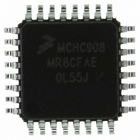
MCHC908MR8CFAE Freescale Semiconductor, MCHC908MR8CFAE Datasheet - Page 64

MCHC908MR8CFAE
Manufacturer Part Number
MCHC908MR8CFAE
Description
IC MCU 8K FLASH 8MHZ PWM 32-LQFP
Manufacturer
Freescale Semiconductor
Series
HC08r
Datasheet
1.MCHC908MR8VFAE.pdf
(372 pages)
Specifications of MCHC908MR8CFAE
Core Processor
HC08
Core Size
8-Bit
Speed
8MHz
Connectivity
SCI
Peripherals
LVD, POR, PWM
Number Of I /o
16
Program Memory Size
8KB (8K x 8)
Program Memory Type
FLASH
Ram Size
256 x 8
Voltage - Supply (vcc/vdd)
4.5 V ~ 5.5 V
Data Converters
A/D 7x10b
Oscillator Type
Internal
Operating Temperature
-40°C ~ 85°C
Package / Case
32-LQFP
Controller Family/series
HC08
No. Of I/o's
16
Ram Memory Size
256Byte
Cpu Speed
8MHz
No. Of Timers
2
Rohs Compliant
Yes
Processor Series
HC08MR
Core
HC08
Data Bus Width
8 bit
Data Ram Size
64 B
Interface Type
SCI, SPI
Maximum Clock Frequency
8 MHz
Number Of Programmable I/os
32
Number Of Timers
4
Operating Supply Voltage
0 V to 5 V
Maximum Operating Temperature
+ 85 C
Mounting Style
SMD/SMT
Development Tools By Supplier
FSICEBASE, M68CBL05CE
Minimum Operating Temperature
- 40 C
On-chip Adc
8 bit, 8 Channel
Lead Free Status / RoHS Status
Lead free / RoHS Compliant
Eeprom Size
-
Lead Free Status / Rohs Status
Details
Available stocks
Company
Part Number
Manufacturer
Quantity
Price
Company:
Part Number:
MCHC908MR8CFAE
Manufacturer:
Freescale Semiconductor
Quantity:
10 000
- Current page: 64 of 372
- Download datasheet (4Mb)
FLASH Memory
4.3.3 Low-Power Modes
4.3.3.1 Wait Mode
Technical Data
64
NOTE:
If all bits are erased, then all of the memory is available for erase and
program. The presence of a voltage V
block protection so that all of the memory, including the block protect
register, is open for program and erase operations.
The WAIT and STOP instructions will place the MCU in a low power-
consumption standby mode.
Putting the MCU into wait mode while the FLASH is in read mode does
not affect the operation of the FLASH memory directly, but there will not
be any memory activity since the CPU is inactive.
The WAIT instruction should never be executed while performing a
program or erase operation on the FLASH. When the MCU is put into
wait mode, the charge pump for the FLASH is disabled so that either a
program or erase operation will not continue. If the memory is in either
program mode (PGM = 1, HVEN = 1) or erase mode (ERASE = 1,
HVEN = 1), then it will remain in that mode during wait.
Exiting from wait must now be done with a reset rather than an interrupt
because if exiting wait with an interrupt, the memory will not be in read
mode and the interrupt vector cannot be read from the memory.
$80 = The entire FLASH memory is protected.
$81 = Protected range: $E040–$FFFF
$82 = Protected range: $E080–$FFFF
$FE = Protected range: $FF80–$FFFF
$FF = Entire FLASH memory is not protected.
START ADDRESS OF
BLOCK PROTECT
↓
Figure 4-4. FLASH Block Protect Address
FLASH Memory
FLASH
↓
1
↓
1
FLBPR VALUE
16-BIT MEMORY ADDRESS
HI
on the IRQ pin will bypass the
MC68HC908MR8 — Rev 4.1
Freescale Semiconductor
0
0
0
0
0
0
Related parts for MCHC908MR8CFAE
Image
Part Number
Description
Manufacturer
Datasheet
Request
R
Part Number:
Description:
Manufacturer:
Freescale Semiconductor, Inc
Datasheet:
Part Number:
Description:
Manufacturer:
Freescale Semiconductor, Inc
Datasheet:
Part Number:
Description:
Manufacturer:
Freescale Semiconductor, Inc
Datasheet:
Part Number:
Description:
Manufacturer:
Freescale Semiconductor, Inc
Datasheet:
Part Number:
Description:
Manufacturer:
Freescale Semiconductor, Inc
Datasheet:
Part Number:
Description:
Manufacturer:
Freescale Semiconductor, Inc
Datasheet:
Part Number:
Description:
Manufacturer:
Freescale Semiconductor, Inc
Datasheet:
Part Number:
Description:
Manufacturer:
Freescale Semiconductor, Inc
Datasheet:
Part Number:
Description:
Manufacturer:
Freescale Semiconductor, Inc
Datasheet:
Part Number:
Description:
Manufacturer:
Freescale Semiconductor, Inc
Datasheet:
Part Number:
Description:
Manufacturer:
Freescale Semiconductor, Inc
Datasheet:
Part Number:
Description:
Manufacturer:
Freescale Semiconductor, Inc
Datasheet:
Part Number:
Description:
Manufacturer:
Freescale Semiconductor, Inc
Datasheet:
Part Number:
Description:
Manufacturer:
Freescale Semiconductor, Inc
Datasheet:
Part Number:
Description:
Manufacturer:
Freescale Semiconductor, Inc
Datasheet:


