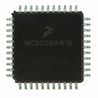
MC9S08AW32CFGE Freescale Semiconductor, MC9S08AW32CFGE Datasheet - Page 104

MC9S08AW32CFGE
Manufacturer Part Number
MC9S08AW32CFGE
Description
IC MCU 32K FLASH 44-LQFP
Manufacturer
Freescale Semiconductor
Series
HCS08r
Specifications of MC9S08AW32CFGE
Core Processor
HCS08
Core Size
8-Bit
Speed
40MHz
Connectivity
I²C, SCI, SPI
Peripherals
LVD, POR, PWM, WDT
Number Of I /o
34
Program Memory Size
32KB (32K x 8)
Program Memory Type
FLASH
Ram Size
2K x 8
Voltage - Supply (vcc/vdd)
2.7 V ~ 5.5 V
Data Converters
A/D 8x10b
Oscillator Type
Internal
Operating Temperature
-40°C ~ 85°C
Package / Case
44-LQFP
Processor Series
S08AW
Core
HCS08
Data Bus Width
8 bit
Data Ram Size
2 KB
Interface Type
I2C, SCI, SPI
Maximum Clock Frequency
40 MHz
Number Of Programmable I/os
34
Number Of Timers
8
Operating Supply Voltage
- 0.3 V to + 5.8 V
Maximum Operating Temperature
+ 85 C
Mounting Style
SMD/SMT
3rd Party Development Tools
EWS08
Development Tools By Supplier
DEMO9S08AW60E
Minimum Operating Temperature
- 55 C
On-chip Adc
10 bit, 8 Channel
Package
44LQFP
Family Name
HCS08
Maximum Speed
40 MHz
Lead Free Status / RoHS Status
Lead free / RoHS Compliant
Eeprom Size
-
Lead Free Status / Rohs Status
Details
Available stocks
Company
Part Number
Manufacturer
Quantity
Price
Company:
Part Number:
MC9S08AW32CFGE
Manufacturer:
FREESCALE
Quantity:
5 456
Company:
Part Number:
MC9S08AW32CFGE
Manufacturer:
Freescale Semiconductor
Quantity:
10 000
Part Number:
MC9S08AW32CFGE
Manufacturer:
FREESCALE
Quantity:
20 000
Company:
Part Number:
MC9S08AW32CFGER
Manufacturer:
Freescale Semiconductor
Quantity:
10 000
- Current page: 104 of 336
- Download datasheet (7Mb)
1
Chapter 6 Parallel Input/Output
6.7.13
Port G parallel I/O function is controlled by the registers listed below.
104
Bits 7, 3 and 2 are reserved bits that must always be written to 0.
PTGD[6:0]
PTFDSn
Reset
Reset
6:4, 1:0
Field
Field
6:0
W
W
R
R
Port G I/O Registers (PTGD and PTGDD)
Output Drive Strength Selection for Port F Bits — Each of these control bits selects between low and high
output drive for the associated PTF pin.
0 Low output drive enabled for port F bit n.
1 High output drive enabled for port F bit n.
Port G Data Register Bits — For port G pins that are inputs, reads return the logic level on the pin. For port G
pins that are configured as outputs, reads return the last value written to this register.
Writes are latched into all bits of this register. For port G pins that are configured as outputs, the logic level is
driven out the corresponding MCU pin.
Reset forces PTGD to all 0s, but these 0s are not driven out the corresponding pins because reset also
configures all port pins as high-impedance inputs with pullups disabled.
R
0
0
0
7
7
Figure 6-39. Output Drive Strength Selection for Port F (PTFDS)
PTFDS6
PTGD6
0
0
6
6
Table 6-30. PTFDS Register Field Descriptions
Table 6-31. PTGD Register Field Descriptions
Figure 6-40. Port G Data Register (PTGD)
PTFDS5
MC9S08AC16 Series Data Sheet, Rev. 8
PTGD5
0
0
5
5
PTFDS4
PTGD4
0
0
4
4
Description
Description
PTGD3
R
3
0
3
0
PTGD2
R
0
0
2
2
1
PTFDS1
Freescale Semiconductor
PTGD1
0
0
1
1
PTFDS0
PTGD0
0
0
0
0
Related parts for MC9S08AW32CFGE
Image
Part Number
Description
Manufacturer
Datasheet
Request
R
Part Number:
Description:
Manufacturer:
Freescale Semiconductor, Inc
Datasheet:
Part Number:
Description:
Manufacturer:
Freescale Semiconductor, Inc
Datasheet:
Part Number:
Description:
Manufacturer:
Freescale Semiconductor, Inc
Datasheet:
Part Number:
Description:
Manufacturer:
Freescale Semiconductor, Inc
Datasheet:
Part Number:
Description:
Manufacturer:
Freescale Semiconductor, Inc
Datasheet:
Part Number:
Description:
Manufacturer:
Freescale Semiconductor, Inc
Datasheet:
Part Number:
Description:
Manufacturer:
Freescale Semiconductor, Inc
Datasheet:
Part Number:
Description:
Manufacturer:
Freescale Semiconductor, Inc
Datasheet:
Part Number:
Description:
Manufacturer:
Freescale Semiconductor, Inc
Datasheet:
Part Number:
Description:
Manufacturer:
Freescale Semiconductor, Inc
Datasheet:
Part Number:
Description:
Manufacturer:
Freescale Semiconductor, Inc
Datasheet:
Part Number:
Description:
Manufacturer:
Freescale Semiconductor, Inc
Datasheet:
Part Number:
Description:
Manufacturer:
Freescale Semiconductor, Inc
Datasheet:
Part Number:
Description:
Manufacturer:
Freescale Semiconductor, Inc
Datasheet:
Part Number:
Description:
Manufacturer:
Freescale Semiconductor, Inc
Datasheet:


