M38039GCHHP#U0 Renesas Electronics America, M38039GCHHP#U0 Datasheet - Page 85
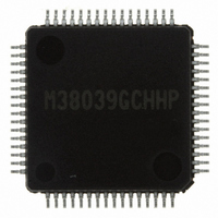
M38039GCHHP#U0
Manufacturer Part Number
M38039GCHHP#U0
Description
IC 740/3803 MCU QZROM 64LQFP
Manufacturer
Renesas Electronics America
Series
740/38000r
Datasheet
1.M38039G4HHPU0.pdf
(105 pages)
Specifications of M38039GCHHP#U0
Core Processor
740
Core Size
8-Bit
Speed
16.8MHz
Connectivity
SIO, UART/USART
Peripherals
LED, PWM, WDT
Number Of I /o
56
Program Memory Size
48KB (48K x 8)
Program Memory Type
QzROM
Ram Size
2K x 8
Voltage - Supply (vcc/vdd)
1.8 V ~ 5.5 V
Data Converters
A/D 16x10b; D/A 2x8b
Oscillator Type
Internal
Operating Temperature
-20°C ~ 85°C
Package / Case
64-LQFP
Lead Free Status / RoHS Status
Lead free / RoHS Compliant
Eeprom Size
-
Available stocks
Company
Part Number
Manufacturer
Quantity
Price


3803 Group (Spec.H QzROM version)
REJ03B0166-0113 Rev.1.13
Page 83 of 100
Notes on 16-bit Timer (timer Z)
1. Pulse output mode
• Set the double-function port of the CNTR
2. Pulse period measurement mode
• Set the double-function port of the CNTR
• A read-out of timer value is impossible in this mode. The timer
• Since the timer latch in this mode is specialized for the read-
• “FFFF
3. Pulse width measurement mode
• Set the double-function port of the CNTR
• A read-out of timer value is impossible in this mode. The timer
• Since the timer latch in this mode is specialized for the read-
• “FFFF
4. Programmable waveform generating mode
• Set the double-function port of the CNTR
5. Programmable one-shot generating mode
• Set the double-function port of CNTR
• This mode cannot be used in low-speed mode.
• If the value of the CNTR
6. All modes
• Timer Z write control
Which write control can be selected by the timer Z write control
bit (bit 3) of the timer Z mode register (address 002A
data to both the latch and the timer at the same time or writing
data only to the latch.
When the operation “writing data only to the latch” is selected,
the value is set to the timer latch by writing data to the address of
timer Z and the timer is updated at next underflow. After reset
release, the operation “writing data to both the latch and the timer
at the same time” is selected, and the value is set to both the latch
and the timer at the same time by writing data to the address of
timer Z.
In the case of writing data only to the latch, if writing data to the
latch and an underflow are performed almost at the same time,
the timer value may become undefined.
output.
input.
can be written to only during timer stop (no measurement of
pulse period).
out of measured values, do not perform any write operation
during measurement.
when the valid edge of measurement start/completion is
detected.
Consequently, the timer value at start of pulse period
measurement depends on the timer value just before
measurement start.
input.
can be written to only during timer stop (no measurement of
pulse period).
out of measured values, do not perform any write operation
during measurement.
when the valid edge of measurement start/completion is
detected.
Consequently, the timer value at start of pulse width
measurement depends on the timer value just before
measurement start.
output.
output, and of INT
during one-shot generating enabled or generating one-shot
pulse, then the output level from CNTR
16
16
” is set to the timer when the timer underflows or
” is set to the timer when the timer underflows or
1
pin and port P4
2
active edge switch bit is changed
2
Aug 21, 2009
to input in this mode.
2
2
pin changes.
2
2
2
2
pin and port P4
pin and port P4
pin and port P4
pin and port P4
pin and port P4
16
), writing
7
7
7
7
7
to
to
to
to
to
• Timer Z read control
A read-out of timer value is impossible in pulse period
measurement mode and pulse width measurement mode. In the
other modes, a read-out of timer value is possible regardless of
count operating or stopped.
However, a read-out of timer latch value is impossible.
• Switch of interrupt active edge of CNTR
Each interrupt active edge depends on setting of the CNTR
active edge switch bit and the INT
• Switch of count source
When switching the count source by the timer Z count source
s e l e c t i o n b i t s , t h e v a l u e o f t i m e r c o u n t i s a l t e r e d i n
inconsiderable amount owing to generating of thin pulses on the
count input signals.
Therefore, select the timer count source before setting the value
to the prescaler and the timer.
Notes on Serial Interface
1. Notes when selecting clock synchronous serial I/O
(1) Stop of transmission operation
As for serial I/Oi (i = 1, 3) that can be used as either a clock
synchronous or an asynchronous (UART) serial I/O, clear the
serial I/Oi enable bit and the transmit enable bit to “0” (serial
I/Oi and transmit disabled).
<Reason>
Since transmission is not stopped and the transmission circuit is
not initialized even if only the serial I/Oi enable bit is cleared to
“0” (serial I/Oi disabled), the internal transmission is running (in
this case, since pins TxDi, RxDi, S
I/O ports, the transmission data is not output). When data is
written to the transmit buffer register i in this state, data starts to
be shifted to the transmit shift register i. When the serial I/Oi
enable bit is set to “1” at this time, the data during internally
shifting is output to the TxDi pin and an operation failure occurs.
(2) Stop of receive operation
As for serial I/Oi (i = 1, 3) that can be used as either a clock
synchronous or an asynchronous (UART) serial I/O, clear the
receive enable bit to “0” (receive disabled), or clear the serial
I/Oi enable bit to “0” (serial I/Oi disabled).
(3) Stop of transmit/receive operation
As for serial I/Oi (i = 1, 3) that can be used as either a clock
synchronous or an asynchronous (UART) serial I/O, clear both
the transmit enable bit and receive enable bit to “0” (transmit and
receive disabled).
(when data is transmitted and received in the clock synchronous
serial I/O mode, any one of data transmission and reception
cannot be stopped.)
<Reason>
In the clock synchronous serial I/O mode, the same clock is used
for transmission and reception. If any one of transmission and
reception is disabled, a bit error occurs because transmission and
reception cannot be synchronized.
In this mode, the clock circuit of the transmission circuit also
operates for data reception. Accordingly, the transmission circuit
does not stop by clearing only the transmit enable bit to “0”
(transmit disabled). Also, the transmission circuit is not
initialized by clearing the serial I/Oi enable bit to “0” (serial I/Oi
disabled) (refer to (1) in 1.).
1
active edge selection bit.
CLK
i, and S
2
and INT
RDY
i function as
1
2
Related parts for M38039GCHHP#U0
Image
Part Number
Description
Manufacturer
Datasheet
Request
R

Part Number:
Description:
KIT STARTER FOR M16C/29
Manufacturer:
Renesas Electronics America
Datasheet:

Part Number:
Description:
KIT STARTER FOR R8C/2D
Manufacturer:
Renesas Electronics America
Datasheet:

Part Number:
Description:
R0K33062P STARTER KIT
Manufacturer:
Renesas Electronics America
Datasheet:

Part Number:
Description:
KIT STARTER FOR R8C/23 E8A
Manufacturer:
Renesas Electronics America
Datasheet:

Part Number:
Description:
KIT STARTER FOR R8C/25
Manufacturer:
Renesas Electronics America
Datasheet:

Part Number:
Description:
KIT STARTER H8S2456 SHARPE DSPLY
Manufacturer:
Renesas Electronics America
Datasheet:

Part Number:
Description:
KIT STARTER FOR R8C38C
Manufacturer:
Renesas Electronics America
Datasheet:

Part Number:
Description:
KIT STARTER FOR R8C35C
Manufacturer:
Renesas Electronics America
Datasheet:

Part Number:
Description:
KIT STARTER FOR R8CL3AC+LCD APPS
Manufacturer:
Renesas Electronics America
Datasheet:
Part Number:
Description:
KIT STARTER FOR RX610
Manufacturer:
Renesas Electronics America
Datasheet:

Part Number:
Description:
KIT STARTER FOR R32C/118
Manufacturer:
Renesas Electronics America
Datasheet:

Part Number:
Description:
KIT DEV RSK-R8C/26-29
Manufacturer:
Renesas Electronics America
Datasheet:

Part Number:
Description:
KIT STARTER FOR SH7124
Manufacturer:
Renesas Electronics America
Datasheet:

Part Number:
Description:
KIT STARTER FOR H8SX/1622
Manufacturer:
Renesas Electronics America
Datasheet:

Part Number:
Description:
KIT DEV FOR SH7203
Manufacturer:
Renesas Electronics America
Datasheet: