R5F363AENFA#U0 Renesas Electronics America, R5F363AENFA#U0 Datasheet - Page 24
R5F363AENFA#U0
Manufacturer Part Number
R5F363AENFA#U0
Description
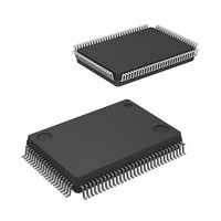
MCU 4KB FLASH 256/16K 100-QFP
Manufacturer
Renesas Electronics America
Series
M16C/60/63r
Specifications of R5F363AENFA#U0
Core Processor
M16C/60
Core Size
16/32-Bit
Speed
20MHz
Connectivity
EBI/EMI, I²C, SIO, UART/USART
Peripherals
DMA, LVD, POR, PWM, WDT
Number Of I /o
85
Program Memory Size
256KB (256K x 8)
Program Memory Type
FLASH
Ram Size
20K x 8
Voltage - Supply (vcc/vdd)
1.8 V ~ 5.5 V
Data Converters
A/D 26x10b; D/A 2x8b
Oscillator Type
Internal
Operating Temperature
-20°C ~ 85°C
Package / Case
100-QFP
Lead Free Status / RoHS Status
Lead free / RoHS Compliant
Eeprom Size
-
Available stocks
Company
Part Number
Manufacturer
Quantity
Price


M16C/63 Group
REJ03B0271-0100 Rev.1.00 Sep 15, 2009
Page 22 of 113
Table 1.14
Note:
Serial interface
UART0 to UART2,
UART5
UART0 to UART2,
UART5
I
Serial interface
SI/O3, SI/O4
Multi-master I
interface
CEC I/O
Reference voltage
input
A/D converter
D/A converter
I/O ports
2
C mode
1.
Signal Name
TXD2, SDA2, and SCL2 are N-channel open drain output pins. TXDi (i = 0, 1, 5), SDAi, and SCLi can be
selected as CMOS output pins or N-channel open drain output pins.
2
C-bus
Pin Functions for the 80-Pin Package (2/2)
AN0_0 to AN0_7
AN2_0 to AN2_7
SOUT3, SOUT4
P10_0 to P10_7
RXD0 to RXD2,
ANEX0, ANEX1
SDA0 to SDA2,
TXD0 to TXD2,
SCL0 to SCL2,
P0_0 to P0_7
P2_0 to P2_7
P3_0 to P3_7
P5_0 to P5_7
P6_0 to P6_7
P8_0 to P8_7
P4_0 to P4_3
P9_2 to P9_7
CTS0, CTS1,
RTS0, RTS1,
CLK0, CLK1,
CLK3, CLK4
AN0 to AN7
P7_0, P7_1
P7_6, P7_7
DA0, DA1
Pin Name
SDAMM
SCLMM
ADTRG
CLKS1
RXD5
VREF
CTS5
RTS5
CLK5
TXD5
SDA5
SCL5
P9_0,
SIN4
CEC
I/O
I/O
I/O
I/O
I/O
I/O
I/O
I/O
I/O
I/O
O
O
O
O
O
I
I
I
I
I
I
I
I
Supply
Power
VCC1
VCC1
VCC1
VCC1
VCC1
VCC1
VCC1
VCC1
VCC1
VCC1
VCC1
VCC1
VCC1
VCC1
VCC1
VCC1
VCC1
VCC1
VCC1
VCC1
VCC1
VCC1
Input pins to control data transmission
Output pins to control data reception
Transmit/receive clock I/O.
Serial data input.
Serial data output.
Output for the transmit/receive clock multiple-pin output
function.
Serial data I/O for I
Transmit/receive clock I/O for I
Serial data input.
Serial data output.
Serial data I/O (N-channel open drain output).
Transmit/receive clock I/O (N-channel open drain output).
CEC I/O (N-channel open drain output).
Reference voltage input for the A/D and D/A converters.
Analog input for the A/D converter.
Input for an external A/D trigger.
Extended analog input for the A/D converter.
Output for the D/A converter.
8-bit CMOS I/O ports. A direction register determines
whether each pin is used as an input port or an output
port. A pull-up resistor may be enabled or disabled for
input ports in 4-bit units. P8_5 is an N-channel open drain
output port. No pull-up resistor is provided. P8_5 is an
input port for verifying the NMI pin level and shares a pin
with NMI.
P7_0 and P7_1 are N-channel open drain output ports.
No pull-up resistor is provided.
Transmit/receive clock I/O.
I/O ports having equivalent functions to P0. However,
(1)
2
C mode.
Description
2
C mode.
1. Overview
Related parts for R5F363AENFA#U0
Image
Part Number
Description
Manufacturer
Datasheet
Request
R

Part Number:
Description:
KIT STARTER FOR M16C/29
Manufacturer:
Renesas Electronics America
Datasheet:

Part Number:
Description:
KIT STARTER FOR R8C/2D
Manufacturer:
Renesas Electronics America
Datasheet:

Part Number:
Description:
R0K33062P STARTER KIT
Manufacturer:
Renesas Electronics America
Datasheet:

Part Number:
Description:
KIT STARTER FOR R8C/23 E8A
Manufacturer:
Renesas Electronics America
Datasheet:

Part Number:
Description:
KIT STARTER FOR R8C/25
Manufacturer:
Renesas Electronics America
Datasheet:

Part Number:
Description:
KIT STARTER H8S2456 SHARPE DSPLY
Manufacturer:
Renesas Electronics America
Datasheet:

Part Number:
Description:
KIT STARTER FOR R8C38C
Manufacturer:
Renesas Electronics America
Datasheet:

Part Number:
Description:
KIT STARTER FOR R8C35C
Manufacturer:
Renesas Electronics America
Datasheet:

Part Number:
Description:
KIT STARTER FOR R8CL3AC+LCD APPS
Manufacturer:
Renesas Electronics America
Datasheet:
Part Number:
Description:
KIT STARTER FOR RX610
Manufacturer:
Renesas Electronics America
Datasheet:

Part Number:
Description:
KIT STARTER FOR R32C/118
Manufacturer:
Renesas Electronics America
Datasheet:

Part Number:
Description:
KIT DEV RSK-R8C/26-29
Manufacturer:
Renesas Electronics America
Datasheet:

Part Number:
Description:
KIT STARTER FOR SH7124
Manufacturer:
Renesas Electronics America
Datasheet:

Part Number:
Description:
KIT STARTER FOR H8SX/1622
Manufacturer:
Renesas Electronics America
Datasheet:

Part Number:
Description:
KIT DEV FOR SH7203
Manufacturer:
Renesas Electronics America
Datasheet: