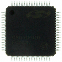
C8051F010-GQ Silicon Laboratories Inc, C8051F010-GQ Datasheet - Page 154

C8051F010-GQ
Manufacturer Part Number
C8051F010-GQ
Description
IC 8051 MCU 32K FLASH 64TQFP
Manufacturer
Silicon Laboratories Inc
Series
C8051F01xr
Specifications of C8051F010-GQ
Core Processor
8051
Core Size
8-Bit
Speed
20MHz
Connectivity
SMBus (2-Wire/I²C), SPI, UART/USART
Peripherals
Brown-out Detect/Reset, POR, PWM, Temp Sensor, WDT
Number Of I /o
32
Program Memory Size
32KB (32K x 8)
Program Memory Type
FLASH
Ram Size
256 x 8
Voltage - Supply (vcc/vdd)
2.7 V ~ 3.6 V
Data Converters
A/D 8x10b; D/A 2x12b
Oscillator Type
Internal
Operating Temperature
-40°C ~ 85°C
Package / Case
64-TQFP, 64-VQFP
Processor Series
C8051F0x
Core
8051
Data Bus Width
8 bit
Data Ram Size
256 B
Interface Type
I2C, SMBus, SPI, UART
Maximum Clock Frequency
20 MHz
Number Of Programmable I/os
32
Number Of Timers
4 bit
Operating Supply Voltage
2.7 V to 3.6 V
Maximum Operating Temperature
+ 85 C
Mounting Style
SMD/SMT
3rd Party Development Tools
PK51, CA51, A51, ULINK2
Development Tools By Supplier
C8051F005DK
Minimum Operating Temperature
- 40 C
On-chip Adc
10 bit, 8 Channel
On-chip Dac
12 bit, 2 Channel
Lead Free Status / RoHS Status
Lead free / RoHS Compliant
Eeprom Size
-
Lead Free Status / Rohs Status
Details
Other names
336-1191
Available stocks
Company
Part Number
Manufacturer
Quantity
Price
Company:
Part Number:
C8051F010-GQ
Manufacturer:
Silicon Laboratories Inc
Quantity:
10 000
20. PROGRAMMABLE COUNTER ARRAY
The Programmable Counter Array (PCA) provides enhanced timer functionality while requiring less CPU
intervention than the standard 8051 counter/timers. The PCA consists of a dedicated 16-bit counter/timer and five
16-bit capture/compare modules. Each capture/compare module has its own associated I/O line (CEXn) which is
routed through the Crossbar to Port I/O when enabled (see Section 15.1 for details on configuring the Crossbar).
The counter/timer is driven by a configurable timebase that can select between four inputs as its source: system
clock divided by twelve, system clock divided by four, Timer 0 overflow, or an external clock signal on the ECI
line. The PCA is configured and controlled through the system controller’s Special Function Registers. The basic
PCA block diagram is shown in Figure 20.1.
T0 Overflow
System
Clock
Capture/Compare
Module 0
/12
/4
CPS=11
10
Figure 20.1. PCA Block Diagram
01
Capture/Compare
00
Module 1
Crossbar
16-Bit Counter/Timer
Rev. 1.7
Port I/O
Capture/Compare
Module 2
C8051F000/1/2/5/6/7
C8051F010/1/2/5/6/7
Capture/Compare
Module 3
Capture/Compare
Module 4
154


