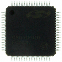
C8051F010-GQ Silicon Laboratories Inc, C8051F010-GQ Datasheet - Page 18

C8051F010-GQ
Manufacturer Part Number
C8051F010-GQ
Description
IC 8051 MCU 32K FLASH 64TQFP
Manufacturer
Silicon Laboratories Inc
Series
C8051F01xr
Specifications of C8051F010-GQ
Core Processor
8051
Core Size
8-Bit
Speed
20MHz
Connectivity
SMBus (2-Wire/I²C), SPI, UART/USART
Peripherals
Brown-out Detect/Reset, POR, PWM, Temp Sensor, WDT
Number Of I /o
32
Program Memory Size
32KB (32K x 8)
Program Memory Type
FLASH
Ram Size
256 x 8
Voltage - Supply (vcc/vdd)
2.7 V ~ 3.6 V
Data Converters
A/D 8x10b; D/A 2x12b
Oscillator Type
Internal
Operating Temperature
-40°C ~ 85°C
Package / Case
64-TQFP, 64-VQFP
Processor Series
C8051F0x
Core
8051
Data Bus Width
8 bit
Data Ram Size
256 B
Interface Type
I2C, SMBus, SPI, UART
Maximum Clock Frequency
20 MHz
Number Of Programmable I/os
32
Number Of Timers
4 bit
Operating Supply Voltage
2.7 V to 3.6 V
Maximum Operating Temperature
+ 85 C
Mounting Style
SMD/SMT
3rd Party Development Tools
PK51, CA51, A51, ULINK2
Development Tools By Supplier
C8051F005DK
Minimum Operating Temperature
- 40 C
On-chip Adc
10 bit, 8 Channel
On-chip Dac
12 bit, 2 Channel
Lead Free Status / RoHS Status
Lead free / RoHS Compliant
Eeprom Size
-
Lead Free Status / Rohs Status
Details
Other names
336-1191
Available stocks
Company
Part Number
Manufacturer
Quantity
Price
Company:
Part Number:
C8051F010-GQ
Manufacturer:
Silicon Laboratories Inc
Quantity:
10 000
1.7.
The C8051F000/1/2/5/6/7 has an on-chip 12-bit SAR ADC with a 9-channel input multiplexer and programmable
gain amplifier. With a maximum throughput of 100ksps, the ADC offers true 12-bit accuracy with an INL of
1LSB. The ADC in the C8051F010/1/2/5/6/7 is similar, but with 10-bit resolution. Each ADC has a maximum
throughput of 100ksps. Each ADC has an INL of 1LSB, offering true 12-bit accuracy with the C8051F00x, and
true 10-bit accuracy with the C8051F01x. There is also an on-board 15ppm voltage reference, or an external
reference may be used via the VREF pin.
The ADC is under full control of the CIP-51 microcontroller via the Special Function Registers. One input channel
is tied to an internal temperature sensor, while the other eight channels are available externally. Each pair of the
eight external input channels can be configured as either two single-ended inputs or a single differential input. The
system controller can also put the ADC into shutdown to save power.
A programmable gain amplifier follows the analog multiplexer. The gain can be set in software from 0.5 to 16 in
powers of 2. The gain stage can be especially useful when different ADC input channels have widely varied input
voltage signals, or when it is necessary to “zoom in” on a signal with a large DC offset (in differential mode, a DAC
could be used to provide the DC offset).
Conversions can be started in four ways; a software command, an overflow on Timer 2, an overflow on Timer 3, or
an external signal input. This flexibility allows the start of conversion to be triggered by software events, external
HW signals, or convert continuously. A completed conversion causes an interrupt, or a status bit can be polled in
software to determine the end of conversion. The resulting 10 or 12-bit data word is latched into two SFRs upon
completion of a conversion. The data can be right or left justified in these registers under software control.
Compare registers for the ADC data can be configured to interrupt the controller when ADC data is within a
specified window. The ADC can monitor a key voltage continuously in background mode, but not interrupt the
controller unless the converted data is within the specified window.
Analog to Digital Converter
(not bonded out on
F002, F007, F012,
and F017
AIN0
AIN1
AIN2
AIN3
AIN4
AIN5
AIN6
AIN7
Figure 1.10. ADC Diagram
+
-
+
-
+
-
+
-
AMUX
9-to-1
(SE or
DIFF)
SENSOR
TEMP
Rev. 1.7
X
Programmable
Gain Amp
+
-
Control & Data
SFR's
REF
SFR Bus
100ksps
ADC
C8051F000/1/2/5/6/7
C8051F010/1/2/5/6/7
SAR
VREF
18


