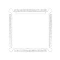
MC68HC16Z1CEH16 Freescale Semiconductor, MC68HC16Z1CEH16 Datasheet - Page 9

MC68HC16Z1CEH16
Manufacturer Part Number
MC68HC16Z1CEH16
Description
IC MCU 16BIT 16MHZ 132-PQFP
Manufacturer
Freescale Semiconductor
Series
HC16r
Specifications of MC68HC16Z1CEH16
Core Processor
CPU16
Core Size
16-Bit
Speed
16MHz
Connectivity
EBI/EMI, SCI, SPI
Peripherals
POR, PWM, WDT
Number Of I /o
16
Program Memory Type
ROMless
Ram Size
1K x 8
Voltage - Supply (vcc/vdd)
2.7 V ~ 5.5 V
Data Converters
A/D 8x10b
Oscillator Type
Internal
Operating Temperature
-40°C ~ 85°C
Package / Case
132-QFP
Processor Series
HC16Z
Core
CPU16
Data Bus Width
16 bit
Controller Family/series
68HC16
No. Of I/o's
26
Ram Memory Size
1KB
Cpu Speed
16MHz
No. Of Timers
2
Embedded Interface Type
QSPI, SCI
Rohs Compliant
Yes
Package
132PQFP
Family Name
HC16
Maximum Speed
16 MHz
Operating Supply Voltage
3.3|5 V
Number Of Programmable I/os
16
On-chip Adc
8-chx10-bit
Number Of Timers
11
Data Ram Size
1 KB
Interface Type
SCI, SPI, UART
Maximum Clock Frequency
16 MHz
Maximum Operating Temperature
+ 85 C
Mounting Style
SMD/SMT
Minimum Operating Temperature
- 40 C
Lead Free Status / RoHS Status
Lead free / RoHS Compliant
Eeprom Size
-
Program Memory Size
-
Lead Free Status / Rohs Status
Lead free / RoHS Compliant
Available stocks
Company
Part Number
Manufacturer
Quantity
Price
Company:
Part Number:
MC68HC16Z1CEH16
Manufacturer:
Freescale Semiconductor
Quantity:
10 000
Part Number:
MC68HC16Z1CEH16
Manufacturer:
FREESCALE
Quantity:
20 000
M68HC16ZEC25/D
Num
NOTES:
100
101
102
103
104
105
1. All AC timing is shown with respect to 20% V
2. Minimum system clock frequency is four times the crystal frequency, subject to specified limits.
3. When an external clock is used, minimum high and low times are based on a 50% duty cycle. The mini-
Minimum t
4. Parameters for an external clock signal applied while the internal PLL is disabled (MODCLK pin held
5. Specification 9A is the worst-case skew between AS and DS or CS. The amount of skew depends on
6. If multiple chip selects are used, CS width negated (specification 15) applies to the time from the nega-
7. Hold times are specified with respect to DS or CS on asynchronous reads and with respect to CLKOUT
8. Maximum value is equal to (t
9. If the asynchronous setup time (specification 47A) requirements are satisfied, the DSACK[1:0] low to
10. To ensure coherency during every operand transfer, BG is not asserted in response to BR until after all
11. In the absence of DSACK[1:0], BERR is an asynchronous input using the asynchronous setup time
12. After external RESET negation is detected, a short transition period (approximately 2 t
13. External assertion of the RESET input can overlap internally-generated resets. To insure that an exter-
14. External logic must pull RESET high during this period in order for normal MCU operation to begin.
15. Eight pipeline states are multiplexed into IPIPE[1:0]. The multiplexed signals have two phases.
16.Address access time = (2.5 + WS) t
mum allowable t
between external clock input duty cycle and minimum t
low during reset). Does not pertain to an external VCO reference applied while the PLL is enabled
(MODCLK pin held high during reset). When the PLL is enabled, the clock synthesizer detects succes-
sive transitions of the reference signal. If transitions occur within the correct clock period, rise/fall times
and duty cycle are not critical.
the relative loading of these signals. When loads are kept within specified limits, skew will not cause AS
and DS to fall outside the limits shown in specification 9.
tion of a heavily loaded chip select to the assertion of a lightly loaded chip select. The CS width negated
specification between multiple chip selects does not apply to chip selects being used for synchronous
ECLK cycles.
on fast cycle reads. The user is free to use either hold time.
data setup time (specification 31) and DSACK[1:0] low to BERR low setup time (specification 48) can be
ignored. The data must only satisfy the data-in to clock low setup time (specification 27) for the following
clock cycle. BERR must satisfy only the late BERR low to clock low setup time (specification 27A) for
the following clock cycle.
cycles of the current operand transfer are complete.
(specification 47A).
then the SIM drives RESET low for 512 tcyc.
nal reset is recognized in all cases, RESET must be asserted for at least 590 CLKOUT cycles.
Chip select access time = (2 + WS) t
Where: WS = number of wait states. When fast termination is used (2 clock bus) WS = –1.
CLKOUT High to Phase 1 Asserted
CLKOUT High to Phase 2 Asserted
Phase 1 Valid to AS or DS Asserted
Phase 2 Valid to AS or DS Asserted
AS or DS Valid to Phase 1 Negated
AS or DS Negated to Phase 2 Negated
Xcyc
period = minimum t
(V
Xcyc
DD
period is reduced when the duty cycle of the external clock varies. The relationship
and V
Freescale Semiconductor, Inc.
For More Information On This Product,
Table A–6 AC Timing (Continued)
Characteristic
DDSYN
cyc
XCHL
/ 2) + 25 ns.
= 5.0 Vdc
Go to: www.freescale.com
cyc
cyc
15
15
15
15
15
/ (50% – external clock input duty cycle tolerance).
– t
– t
15
CHAV
CLSA
DD
and 70% V
– t
– t
5%, V
DICL
DICL
Xcyc
SS
DD
is expressed:
= 0 Vdc, T
levels unless otherwise noted.
Symbol
A
t
t
t
t
t
t
CHP1A
CHP2A
SNP2N
P1VSA
P2VSN
SAP1N
= T
L
to T
H
Min
)
3
3
9
9
9
9
1
cyc
Max
) elapses,
34
34
MOTOROLA
—
—
—
—
Unit
ns
ns
ns
ns
ns
ns
9


