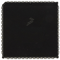
MC68HC711E9CFNE2 Freescale Semiconductor, MC68HC711E9CFNE2 Datasheet - Page 324

MC68HC711E9CFNE2
Manufacturer Part Number
MC68HC711E9CFNE2
Description
IC MCU 8BIT 512RAM 52-PLC
Manufacturer
Freescale Semiconductor
Series
HC11r
Datasheet
1.MC68HC711E9CFNE3.pdf
(336 pages)
Specifications of MC68HC711E9CFNE2
Core Processor
HC11
Core Size
8-Bit
Speed
2MHz
Connectivity
SCI, SPI
Peripherals
POR, WDT
Number Of I /o
38
Program Memory Size
12KB (12K x 8)
Program Memory Type
OTP
Eeprom Size
512 x 8
Ram Size
512 x 8
Voltage - Supply (vcc/vdd)
4.5 V ~ 5.5 V
Data Converters
A/D 8x8b
Oscillator Type
Internal
Operating Temperature
-40°C ~ 85°C
Package / Case
52-PLCC
Processor Series
HC711E
Core
HC11
Data Bus Width
8 bit
Data Ram Size
512 B
Interface Type
SCI, SPI
Maximum Clock Frequency
2 MHz
Number Of Programmable I/os
38
Number Of Timers
8
Maximum Operating Temperature
+ 85 C
Mounting Style
SMD/SMT
Minimum Operating Temperature
- 40 C
On-chip Adc
8 bit
Lead Free Status / RoHS Status
Lead free / RoHS Compliant
Available stocks
Company
Part Number
Manufacturer
Quantity
Price
Company:
Part Number:
MC68HC711E9CFNE2
Manufacturer:
TE
Quantity:
12 000
Company:
Part Number:
MC68HC711E9CFNE2
Manufacturer:
FREESCAL
Quantity:
5 530
- Current page: 324 of 336
- Download datasheet (4Mb)
Engineering Bulletin
To Execute the Program
Step 1
Step 2
324
Use this step-by-step procedure to program the MC68HC711E9 device.
Apply power to the programmer board by moving the +5-V switch to the
ON position. From a DOS command line prompt, start PCbug11this way:
PCbug11 only supports COM ports 1 and 2. If the proper connections
are made and you have a high-quality cable, you should quickly get a
•
•
•
•
•
•
C:\PCBUG11\ > PCBUG11 –E PORT = 1
C:\PCBUG11\ > PCBUG11 –E PORT = 2
with the E9PGMR connected to COM2
with the E9PGMR connected to COM1
Before applying power to the programming board, connect the
M68HC711E9PGMR serial port P2 to one of your PC COM ports
with a standard 25-pin RS-232 cable. Do not use a null modem
cable or adapter which swaps the transmit and receive signals
between the connectors at each end of the cable.
Place the MC68HC711E9 part in the PLCC socket on your board.
Insert the part upside down with the notched corner pointing
toward the red power LED.
Make sure both S1 and S2 switches are turned off.
Apply +5 volts to +5-V, +12 volts (at most +12.5 volts) to V
ground to GND on your programmer board’s power connector, P1.
The remaining TXD/PD1 and RXD/PD0 connections are not used
in this procedure. They are for gang programming MC68HC711E9
devices, which is discussed in the M68HC711E9PGMR Manual.
You cannot gang program with PCbug11.
Ensure that the "remove for multi-programming" jumper, J1, below
the +5-V power switch has a fabricated jumper installed.
or
MOTOROLA
PP
EB184
, and
Related parts for MC68HC711E9CFNE2
Image
Part Number
Description
Manufacturer
Datasheet
Request
R

Part Number:
Description:
APPENDIX A ELECTRICAL CHARACTERISTICS
Manufacturer:
FREESCALE [Freescale Semiconductor, Inc]
Datasheet:
Part Number:
Description:
Manufacturer:
Freescale Semiconductor, Inc
Datasheet:
Part Number:
Description:
Manufacturer:
Freescale Semiconductor, Inc
Datasheet:
Part Number:
Description:
Manufacturer:
Freescale Semiconductor, Inc
Datasheet:
Part Number:
Description:
Manufacturer:
Freescale Semiconductor, Inc
Datasheet:
Part Number:
Description:
Manufacturer:
Freescale Semiconductor, Inc
Datasheet:
Part Number:
Description:
Manufacturer:
Freescale Semiconductor, Inc
Datasheet:
Part Number:
Description:
Manufacturer:
Freescale Semiconductor, Inc
Datasheet:
Part Number:
Description:
Manufacturer:
Freescale Semiconductor, Inc
Datasheet:
Part Number:
Description:
Manufacturer:
Freescale Semiconductor, Inc
Datasheet:
Part Number:
Description:
Manufacturer:
Freescale Semiconductor, Inc
Datasheet:
Part Number:
Description:
Manufacturer:
Freescale Semiconductor, Inc
Datasheet:
Part Number:
Description:
Manufacturer:
Freescale Semiconductor, Inc
Datasheet:
Part Number:
Description:
Manufacturer:
Freescale Semiconductor, Inc
Datasheet:
Part Number:
Description:
Manufacturer:
Freescale Semiconductor, Inc
Datasheet:


