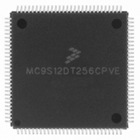
MC9S12DT256CPVE Freescale Semiconductor, MC9S12DT256CPVE Datasheet - Page 2

MC9S12DT256CPVE
Manufacturer Part Number
MC9S12DT256CPVE
Description
IC MCU 256K FLASH 25MHZ 112-LQFP
Manufacturer
Freescale Semiconductor
Series
HCS12r
Datasheet
1.MC9S12DT256MFUE.pdf
(14 pages)
Specifications of MC9S12DT256CPVE
Core Processor
HCS12
Core Size
16-Bit
Speed
25MHz
Connectivity
CAN, I²C, SCI, SPI
Peripherals
PWM, WDT
Number Of I /o
91
Program Memory Size
256KB (256K x 8)
Program Memory Type
FLASH
Eeprom Size
4K x 8
Ram Size
12K x 8
Voltage - Supply (vcc/vdd)
2.35 V ~ 5.25 V
Data Converters
A/D 8x10b
Oscillator Type
Internal
Operating Temperature
-40°C ~ 85°C
Package / Case
112-LQFP
Processor Series
S12D
Core
HCS12
Data Bus Width
16 bit
Data Ram Size
12000 B
Interface Type
I2C, SCI, SPI, CAN
Maximum Clock Frequency
25 MHz
Number Of Programmable I/os
91
Number Of Timers
1
Operating Supply Voltage
- 0.3 V to + 6 V
Maximum Operating Temperature
+ 85 C
Mounting Style
SMD/SMT
3rd Party Development Tools
EWHCS12
Development Tools By Supplier
M68KIT912DP256
Minimum Operating Temperature
- 40 C
On-chip Adc
10 bit
Lead Free Status / RoHS Status
Lead free / RoHS Compliant
Available stocks
Company
Part Number
Manufacturer
Quantity
Price
Company:
Part Number:
MC9S12DT256CPVE
Manufacturer:
Freescale Semiconductor
Quantity:
10 000
• Analog-to-Digital Converters
• Up to five 1M bit per second, CAN 2.0 A, B software compatible modules
• Enhanced Capture Timer (ECT)
• 8 PWM channels with programmable period and duty cycle (7 channels on 80 Pin Packages)
• Serial interfaces
• SAE J1850 Compatible Module (BDLC)
• SIM (System Integration Module)
• Clock generation
• Operating frequency for ambient temperatures T
• Internal 5V to 2.5V Regulator
• 112-Pin LQFP or 80-Pin QFP package
• Development support
2
— One or two 8-channel modules with 10-bit resolution depending on the package option
— External conversion trigger capability
— Five receive and three transmit buffers
— Flexible identifier filter programmable as 2 x 32 bit, 4 x 16 bit or 8 x 8 bit
— Four separate interrupt channels for Receive, Transmit, Error and Wake-up
— Low-pass filter wake-up function in STOP mode
— Loop-back for self test operation
— 16-bit main counter with 7-bit prescaler
— 8 programmable input capture or output compare channels; 4 of the 8 input captures with buffer
— Input capture filters and buffers, three successive captures on four channels, or two captures on four
— Four 8-bit or two 16-bit pulse accumulators
— 16-bit modulus down-counter with 4-bit prescaler
— Four user-selectable delay counters for signal filtering
— 8-bit, 8-channel or 16-bit, 4-channel
— Separate control for each pulse width and duty cycle
— Center- or left-aligned outputs
— Programmable clock select logic with a wide range of frequencies
— Two asynchronous serial communications interfaces (SCI)
— Up to three synchronous serial peripheral interfaces (SPI)
— IIC
— 10.4 kbps Variable Pulse Width format
— Byte level receive and transmit
— 4x receive mode supported
— CRG (windowed COP watchdog, real time interrupt, clock monitor, clock generation and reset)
— MEBI (multiplexed external bus interface)
— INT (interrupt control)
— Phase-locked loop clock frequency multiplier
— Limp home mode in absence of external clock
— Clock Monitor
— Low power 0.5 to 16 MHz crystal oscillator reference clock
— 50MHz equivalent to 25MHz Bus Speed for single chip
— I/O lines with 5V input and drive capability
— 5V A/D converter inputs and 5V I/O
— 2.5V logic supply
— Single-wire background debug™ mode (BDM)
— On-chip hardware breakpoints
channels with a capture/compare selectable on the remaining four
40MHz equivalent to 20MHz Bus Speed in expanded bus modes.
Freescale Semiconductor, Inc.
For More Information On This Product,
Go to: www.freescale.com
A
-40°C <= T
PRODUCT PROPOSAL, Rev 6.1, 23-Oct-02
A
<= 125°C
MC9S


