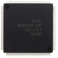
M30835FJGP#U3 Renesas Electronics America, M30835FJGP#U3 Datasheet - Page 23

M30835FJGP#U3
Manufacturer Part Number
M30835FJGP#U3
Description
IC M32C/83 MCU FLASH 144LQFP
Manufacturer
Renesas Electronics America
Series
M16C™ M32C/80r
Datasheets
1.M3087BFLGPU3.pdf
(364 pages)
2.M30833FJGPU3.pdf
(96 pages)
3.M30833FJGPU3.pdf
(529 pages)
Specifications of M30835FJGP#U3
Core Processor
M32C/80
Core Size
16/32-Bit
Speed
32MHz
Connectivity
CAN, I²C, IEBus, SIO, UART/USART
Peripherals
DMA, WDT
Number Of I /o
121
Program Memory Size
512KB (512K x 8)
Program Memory Type
FLASH
Ram Size
31K x 8
Voltage - Supply (vcc/vdd)
3 V ~ 5.5 V
Data Converters
A/D 34x10b, D/A 2x8b
Oscillator Type
Internal
Operating Temperature
-40°C ~ 85°C
Package / Case
144-LQFP
For Use With
R0K330879S001BE - KIT DEV RSK M32C/87R0K330879S000BE - KIT DEV RSK M32C/87
Lead Free Status / RoHS Status
Lead free / RoHS Compliant
Eeprom Size
-
Available stocks
Company
Part Number
Manufacturer
Quantity
Price
R
R
M
e
E
3. Memory
3
. v
J
Figure 3.1 Memory Map
2
0
Figure 3.1 shows a memory map of the M32C/83 group (M32C/83, M32C/83T).
M32C/83 group (M32C/83, M32C/83T) provides 16-Mbyte address space from addresses 000000
FFFFFF
The internal ROM is allocated lower addresses beginning with address FFFFFF
Kbyte internal ROM is allocated addresses FF0000
The fixed interrupt vectors are allocated addresses FFFFDC
of each interrupt routine. Refer to 10. Interrupts for details.
The internal RAM is allocated higher addresses beginning with address 000400
Kbyte internal RAM is allocated addresses 000400
when the subroutine is called or an interrupt is acknowledged.
SFR, consisting of control registers for peripheral functions such as I/O port, A/D conversion, serial I/O, and
timers, is allocated addresses 000000
SFR, are reserved space and cannot be accessed by users.
The special page vectors are allocated addresses FFFE00
tion and JSRS instruction. Refer to the Renesas publication Software Manual for details.
In memory expansion mode and microprocessor mode, some space are reserved and cannot be accessed
by users.
1
3
C
4 .
B
8 /
0
1
0
3
1
J
G
3
a
0 -
n
o r
16
3 .
1
u
, 1
4
.
p
NOTES:
1
2
(
1. In memory expansion and microprocessor modes
2. In memory expansion mode. This space becomes external space in microprocessor mode.
3. This space can be used in single-chip mode and memory expansion mode. This space becomes external
4. Watchdog timer interrupt, oscillation stop detection interrupt, and low voltage detection interrupt share vectors.
M
0
000000
000400
007FFF
008000
F00000
F80000
FFFFFF
space in microprocessor mode.
0
3
6
2
C
8 /
16
16
16
16
16
Page 21
16
16
, 3
M
Reserved Space
Reserved Space
External Space
Internal RAM
Internal ROM
3
2
C
SFR
f o
8 /
9
3
1
) T
(3)
(1)
(2)
16
to 0003FF
FFFFDC
FFFFFF
FFFE00
16
16
16
16
16
16
to 002BFF
Undefined Instruction
. All addresses, which have nothing allocated within
Watchdog Timer
to FFFFFF
BRK Instruction
Address Match
Special Page
Vector Table
Overflow
Reset
16
NMI
16
to FFFFDB
to FFFFFF
16
16
. Besides storing data, it becomes stacks
(4)
.
16
16
. It is used for the JMPS instruc-
. It stores the starting address
16
16
. For example, a 10-
. For example, a 64-
16
to


