M30624FGAFP#U3 Renesas Electronics America, M30624FGAFP#U3 Datasheet - Page 22
M30624FGAFP#U3
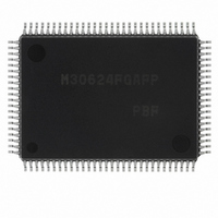
Manufacturer Part Number
M30624FGAFP#U3
Description
IC M16C MCU FLASH 100QFP
Manufacturer
Renesas Electronics America
Series
M16C™ M16C/60r
Datasheets
1.M30622SAFPU5.pdf
(277 pages)
2.M30622SAFPU5.pdf
(617 pages)
3.M30622SAFPU5.pdf
(308 pages)
Specifications of M30624FGAFP#U3
Core Processor
M16C/60
Core Size
16-Bit
Speed
16MHz
Connectivity
SIO, UART/USART
Peripherals
DMA, PWM, WDT
Number Of I /o
85
Program Memory Size
256KB (256K x 8)
Program Memory Type
FLASH
Ram Size
20K x 8
Voltage - Supply (vcc/vdd)
4.2 V ~ 5.5 V
Data Converters
A/D 10x10b, D/A 2x8b
Oscillator Type
Internal
Operating Temperature
-40°C ~ 85°C
Package / Case
100-QFP
For Use With
867-1000 - KIT QUICK START RENESAS 62PM3062PT3-CPE-3 - EMULATOR COMPACT M16C/62P/30P
Lead Free Status / RoHS Status
Lead free / RoHS Compliant
Eeprom Size
-
Available stocks
Company
Part Number
Manufacturer
Quantity
Price

Part Number:
M30624FGAFP#U3M30624FGAFP#D3
Manufacturer:
Renesas Electronics America
Quantity:
10 000
Part Number:
M30624FGAFP#U3M30624FGAFP#D5
Manufacturer:
Renesas Electronics America
Quantity:
10 000


1.3 Register Configuration
Chapter 1 Overview
The central processing unit (CPU) contains the 13 registers shown in Figure 1.3.1. Of these registers, R0,
R1, R2, R3, A0, A1, and FB each consist of two sets of registers configuring two register banks.
Figure 1.3.1 CPU register configuration
1.3.1 Data registers (R0, R0H, R0L, R1, R1H, R1L, R2, and R3)
*1
The data registers (R0, R1, R2, and R3) consist of 16 bits, and are used primarily for transfers and
arithmetic/logic operations.
Registers R0 and R1 can be halved into separate high-order (R0H, R1H) and low-order (R0L, R1L) parts
for use as 8-bit data registers. For some instructions, moreover, you can combine R2 and R0 or R3 and
R1 to configure a 32-bit data register (R2R0 or R3R1).
R0
R1
R2
R3
A0
A1
FB
These registers have two register banks.
*1
*1
*1
*1
*1
*1
*1
b15
b15
b15
b15
b15
b15
b15
H
H
b8b7
b8b7
L
L
IPL
b0
b0
b0
b0
b0
b0
b0
Frame
base
register
Data
registers
Address
registers
PC
INTB H
U I O B S Z D C
4
USP
ISP
SB
FLG
b19
b19
b15
b15
b15
b15
L
1.3 Register Configuration
b0
b0
b0
b0
b0
b0
Program
counter
Interrupt table
register
User stack
pointer
Interrupt stack
pointer
Static base
register
Flag register
Related parts for M30624FGAFP#U3
Image
Part Number
Description
Manufacturer
Datasheet
Request
R

Part Number:
Description:
KIT STARTER FOR M16C/29
Manufacturer:
Renesas Electronics America
Datasheet:

Part Number:
Description:
KIT STARTER FOR R8C/2D
Manufacturer:
Renesas Electronics America
Datasheet:

Part Number:
Description:
R0K33062P STARTER KIT
Manufacturer:
Renesas Electronics America
Datasheet:

Part Number:
Description:
KIT STARTER FOR R8C/23 E8A
Manufacturer:
Renesas Electronics America
Datasheet:

Part Number:
Description:
KIT STARTER FOR R8C/25
Manufacturer:
Renesas Electronics America
Datasheet:

Part Number:
Description:
KIT STARTER H8S2456 SHARPE DSPLY
Manufacturer:
Renesas Electronics America
Datasheet:

Part Number:
Description:
KIT STARTER FOR R8C38C
Manufacturer:
Renesas Electronics America
Datasheet:

Part Number:
Description:
KIT STARTER FOR R8C35C
Manufacturer:
Renesas Electronics America
Datasheet:

Part Number:
Description:
KIT STARTER FOR R8CL3AC+LCD APPS
Manufacturer:
Renesas Electronics America
Datasheet:
Part Number:
Description:
KIT STARTER FOR RX610
Manufacturer:
Renesas Electronics America
Datasheet:

Part Number:
Description:
KIT STARTER FOR R32C/118
Manufacturer:
Renesas Electronics America
Datasheet:

Part Number:
Description:
KIT DEV RSK-R8C/26-29
Manufacturer:
Renesas Electronics America
Datasheet:

Part Number:
Description:
KIT STARTER FOR SH7124
Manufacturer:
Renesas Electronics America
Datasheet:

Part Number:
Description:
KIT STARTER FOR H8SX/1622
Manufacturer:
Renesas Electronics America
Datasheet:

Part Number:
Description:
KIT DEV FOR SH7203
Manufacturer:
Renesas Electronics America
Datasheet: