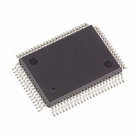
DS5003FPM-16+ Maxim Integrated Products, DS5003FPM-16+ Datasheet - Page 13

DS5003FPM-16+
Manufacturer Part Number
DS5003FPM-16+
Description
IC MICROPROCESSOR SECURE 80-MQFP
Manufacturer
Maxim Integrated Products
Series
DS500xr
Datasheet
1.DS5003-CS1.pdf
(24 pages)
Specifications of DS5003FPM-16+
Core Processor
8051
Core Size
8-Bit
Speed
16MHz
Connectivity
EBI/EMI, SIO, UART/USART
Peripherals
Power-Fail Reset, WDT
Number Of I /o
32
Program Memory Type
SRAM
Ram Size
256 x 8
Voltage - Supply (vcc/vdd)
4 V ~ 5.5 V
Oscillator Type
External
Operating Temperature
0°C ~ 70°C
Package / Case
80-MQFP, 80-PQFP
Processor Series
DS5003
Core
8051
Data Bus Width
8 bit
Program Memory Size
32 KB, 64 KB, 128 KB
Data Ram Size
32 KB, 64 KB, 128 KB
Interface Type
UART
Maximum Clock Frequency
16 MHz
Number Of Programmable I/os
32
Number Of Timers
2
Operating Supply Voltage
4.5 V to 5.5 V
Maximum Operating Temperature
+ 70 C
Mounting Style
SMD/SMT
3rd Party Development Tools
PK51, CA51, A51, ULINK2
Minimum Operating Temperature
0 C
Lead Free Status / RoHS Status
Lead free / RoHS Compliant
Eeprom Size
-
Program Memory Size
-
Data Converters
-
Lead Free Status / Rohs Status
Details
PIN
37
35
33
30
28
26
24
20
76
80
18
16
55
57
59
61
65
67
69
71
70
10
74
72
63
6
4
8
2
______________________________________________________________________________________
NAME
BA10
BA11
BA12
BA13
BA14
CE1N
BA0
BA1
BA2
BA3
BA4
BA5
BA6
BA7
BA8
BA9
BD0
BD1
BD2
BD3
BD4
BD5
BD6
BD7
ALE
R/W
CE1
CE2
CE3
Byte-Wide Address Bus Bits 14–0. This bus is combined with the nonmultiplexed data bus
(BD7–BD0) to access external SRAM. Decoding is performed using CE1–CE4. Therefore, BA15
is not actually needed. Read/write access is controlled by R/W. BA14–BA0 connect directly to
an 8kB, 32kB, or 128kB SRAM. If an 8kB SRAM is used, BA13 and BA14 are unconnected. If a
128kB SRAM is used, the microcontroller converts CE2 and CE3 to serve as A16 and A15,
respectively.
Byte-Wide Data Bus Bits 7–0. This 8-bit bidirectional bus is combined with the nonmultiplexed
address bus (BA14–BA0) to access external SRAM. Decoding is performed on CE1 and CE2.
Read/write access is controlled by R/W. D7–D0 connect directly to an SRAM and optionally to a
real-time clock or other peripheral.
Address Latch Enable. Used to demultiplex the multiplexed expanded address/data bus on port
0. This pin is normally connected to the clock input on a ’373 type transparent latch.
Read/Write (Active Low). This signal provides the write enable to the SRAMs on the byte-wide
bus. It is controlled by the memory map and partition. The blocks selected as program (ROM)
are write protected.
Active-Low Chip-Enable 1. This is the primary decoded chip enable for memory access on the
byte-wide bus. It connects to the chip-enable input of one SRAM. CE1 is lithium-backed. It
remains in a logic-high inactive state when V
Nonbattery-Backed Version of CE1. It is not generally useful because the DS5003 cannot be
used with EPROM due to its encryption.
Active-Low Chip-Enable 2. This chip enable is provided to access a second 32kB block of
memory. It connects to the chip-enable input of one SRAM. When MSEL = 0, the microcontroller
converts CE2 into A16 for a 128kB x 8 SRAM. CE2 is lithium-backed and remains at a logic-high
when V
Active-Low Chip-Enable 3. This chip enable is provided to access a third 32kB block of
memory. It connects to the chip-enable input of one SRAM. When MSEL = 0, the microcontroller
converts CE3 into A15 for a 128kB x 8 SRAM. CE3 is lithium backed and remains at a logic-high
when V
CC
CC
falls below V
falls below V
BYTE-WIDE BUS INTERFACE PINS
Secure Microprocessor Chip
LI
LI
.
.
FUNCTION
CC
Pin Description (continued)
falls below V
LI
.
13


