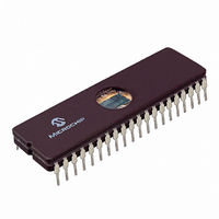
PIC16C64A/JW Microchip Technology, PIC16C64A/JW Datasheet - Page 58

PIC16C64A/JW
Manufacturer Part Number
PIC16C64A/JW
Description
IC MCU EPROM 2KX14 PWM 40CDIP
Manufacturer
Microchip Technology
Series
PIC® 16Cr
Datasheets
1.PIC16F616T-ISL.pdf
(8 pages)
2.PIC16F818-ISO.pdf
(6 pages)
3.PIC16LC62A-04SP.pdf
(337 pages)
4.PIC16C64A-04P.pdf
(8 pages)
Specifications of PIC16C64A/JW
Core Processor
PIC
Core Size
8-Bit
Speed
20MHz
Connectivity
I²C, SPI
Peripherals
Brown-out Detect/Reset, POR, PWM, WDT
Number Of I /o
33
Program Memory Size
3.5KB (2K x 14)
Program Memory Type
EPROM, UV
Ram Size
128 x 8
Voltage - Supply (vcc/vdd)
4 V ~ 6 V
Oscillator Type
External
Operating Temperature
0°C ~ 70°C
Package / Case
40-CDIP (0.600", 15.24mm) Window
For Use With
444-1001 - DEMO BOARD FOR PICMICRO MCU
Lead Free Status / RoHS Status
Lead free / RoHS Compliant
Eeprom Size
-
Data Converters
-
Other names
PIC16C64A/JWR
PIC16C64A/JWR
PIC16C64A/JWR
Available stocks
Company
Part Number
Manufacturer
Quantity
Price
Company:
Part Number:
PIC16C64A/JW
Manufacturer:
Microchip Technology
Quantity:
55
- PIC16F616T-ISL PDF datasheet
- PIC16F818-ISO PDF datasheet #2
- PIC16LC62A-04SP PDF datasheet #3
- PIC16C64A-04P PDF datasheet #4
- Current page: 58 of 337
- Download datasheet (3Mb)
PIC16C6X
5.5
PORTE has three pins, RE2/CS, RE1/WR, and
RE0/RD which are individually configurable as inputs
or outputs. These pins have Schmitt Trigger input buff-
ers.
I/O PORTE becomes control inputs for the micropro-
cessor port when bit PSPMODE (TRISE<4>) is set. In
this mode, the user must make sure that the
TRISE<2:0> bits are set (pins are configured as digital
inputs). In this mode the input buffers are TTL.
Figure 5-9 shows the TRISE register, which controls
the parallel slave port operation and also controls the
direction of the PORTE pins.
FIGURE 5-9:
DS30234D-page 58
Applicable Devices
61 62 62A R62 63 R63 64 64A R64 65 65A R65 66 67
bit7
bit 7 :
bit 6:
bit 5:
bit 4:
bit 3:
bit 2:
bit 1:
bit 0:
R-0
IBF
PORTE and TRISE Register
IBF: Input Buffer Full Status bit
1 = A word has been received and is waiting to be read by the CPU
0 = No word has been received
OBF: Output Buffer Full Status bit
1 = The output buffer still holds a previously written word
0 = The output buffer has been read
IBOV: Input Buffer Overflow Detect bit (in microprocessor mode)
1 = A write occurred when a previously input word has not been read (must be cleared in software)
0 = No overflow occurred
PSPMODE: Parallel Slave Port Mode Select bit
1 = Parallel slave port mode
0 = General purpose I/O mode
Unimplemented: Read as '0'
PORTE Data Direction Bits
Bit2: Direction Control bit for pin RE2/CS
1 = Input
0 = Output
Bit1: Direction Control bit for pin RE1/WR
1 = Input
0 = Output
Bit0: Direction Control bit for pin RE0/RD
1 = Input
0 = Output
OBF
R-0
TRISE REGISTER (ADDRESS 89h)
R/W-0
IBOV
PSPMODE
R/W-0
U-0
—
R/W-1
bit2
FIGURE 5-8:
Note 1: I/O pins have protection diodes to V
R/W-1
bit1
Data
bus
WR
TRIS
WR
PORT
RD PORT
R/W-1
TRIS Latch
Data Latch
bit0
D
D
CK
CK
bit0
RD TRIS
PORTE BLOCK DIAGRAM
(IN I/O PORT MODE)
Q
Q
R = Readable bit
W = Writable bit
U = Unimplemented bit,
- n = Value at POR reset
1997 Microchip Technology Inc.
Q
read as ‘0’
EN
Schmitt
Trigger
input
buffer
EN
D
DD
I/O pin
and V
SS
(1)
.
Related parts for PIC16C64A/JW
Image
Part Number
Description
Manufacturer
Datasheet
Request
R

Part Number:
Description:
MICRO CTRL 2K X 14 OTP 40 DIP
Manufacturer:
Microchip Technology
Datasheet:

Part Number:
Description:
MICRO CTRL 2K X 14 OTP 40 DIP
Manufacturer:
Microchip Technology
Datasheet:

Part Number:
Description:
MICRO CTRL 2K X 14 OTP 44 PLCC
Manufacturer:
Microchip Technology
Datasheet:

Part Number:
Description:
MICRO CTRL 2K X 14 EPROM 40 CDIP
Manufacturer:
Microchip Technology
Datasheet:

Part Number:
Description:
MICRO CTRL 2K X 14 OTP 44 PLCC
Manufacturer:
Microchip Technology
Datasheet:

Part Number:
Description:
MICRO CTRL 2K X 14 OTP 40 DIP
Manufacturer:
Microchip Technology
Datasheet:

Part Number:
Description:
MICRO CTRL 2K X 14 OTP 44 PLCC
Manufacturer:
Microchip Technology
Datasheet:

Part Number:
Description:
IC MCU 2K 20MHZ OTP IT 40DIP
Manufacturer:
Microchip Technology
Datasheet:

Part Number:
Description:
8-Bit CMOS Microcontrollers
Manufacturer:
Microchip Technology
Datasheet:

Part Number:
Description:
8-Bit CMOS Microcontrollers
Manufacturer:
Microchip Technology

Part Number:
Description:
8-Bit CMOS Microcontrollers
Manufacturer:
Microchip Technology

Part Number:
Description:
8-Bit CMOS Microcontrollers
Manufacturer:
Microchip Technology

Part Number:
Description:
8-Bit CMOS Microcontrollers
Manufacturer:
Microchip Technology

Part Number:
Description:
8-Bit CMOS Microcontrollers
Manufacturer:
Microchip Technology

Part Number:
Description:
8-Bit CMOS Microcontrollers
Manufacturer:
Microchip Technology


