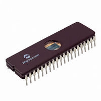
PIC16C64A/JW Microchip Technology, PIC16C64A/JW Datasheet - Page 89

PIC16C64A/JW
Manufacturer Part Number
PIC16C64A/JW
Description
IC MCU EPROM 2KX14 PWM 40CDIP
Manufacturer
Microchip Technology
Series
PIC® 16Cr
Datasheets
1.PIC16F616T-ISL.pdf
(8 pages)
2.PIC16F818-ISO.pdf
(6 pages)
3.PIC16LC62A-04SP.pdf
(337 pages)
4.PIC16C64A-04P.pdf
(8 pages)
Specifications of PIC16C64A/JW
Core Processor
PIC
Core Size
8-Bit
Speed
20MHz
Connectivity
I²C, SPI
Peripherals
Brown-out Detect/Reset, POR, PWM, WDT
Number Of I /o
33
Program Memory Size
3.5KB (2K x 14)
Program Memory Type
EPROM, UV
Ram Size
128 x 8
Voltage - Supply (vcc/vdd)
4 V ~ 6 V
Oscillator Type
External
Operating Temperature
0°C ~ 70°C
Package / Case
40-CDIP (0.600", 15.24mm) Window
For Use With
444-1001 - DEMO BOARD FOR PICMICRO MCU
Lead Free Status / RoHS Status
Lead free / RoHS Compliant
Eeprom Size
-
Data Converters
-
Other names
PIC16C64A/JWR
PIC16C64A/JWR
PIC16C64A/JWR
Available stocks
Company
Part Number
Manufacturer
Quantity
Price
Company:
Part Number:
PIC16C64A/JW
Manufacturer:
Microchip Technology
Quantity:
55
- PIC16F616T-ISL PDF datasheet
- PIC16F818-ISO PDF datasheet #2
- PIC16LC62A-04SP PDF datasheet #3
- PIC16C64A-04P PDF datasheet #4
- Current page: 89 of 337
- Download datasheet (3Mb)
11.3
This section contains register definitions and opera-
tional characterisitics of the SPI module on the
PIC16C66 and PIC16C67 only.
FIGURE 11-7: SSPSTAT: SYNC SERIAL PORT STATUS REGISTER (ADDRESS 94h)(PIC16C66/67)
1997 Microchip Technology Inc.
bit7
bit 7:
bit 6:
bit 5:
bit 4:
bit 3:
bit 2:
bit 1:
bit 0:
R/W-0 R/W-0
SMP
SPI Mode for PIC16C66/67
SMP: SPI data input sample phase
SPI Master Mode
1 = Input data sampled at end of data output time
0 = Input data sampled at middle of data output time
SPI Slave Mode
SMP must be cleared when SPI is used in slave mode
CKE: SPI Clock Edge Select (Figure 11-11, Figure 11-12, and Figure 11-13)
CKP = 0
1 = Data transmitted on rising edge of SCK
0 = Data transmitted on falling edge of SCK
CKP = 1
1 = Data transmitted on falling edge of SCK
0 = Data transmitted on rising edge of SCK
D/A: Data/Address bit (I
1 = Indicates that the last byte received or transmitted was data
0 = Indicates that the last byte received or transmitted was address
P: Stop bit (I
detected last, SSPEN is cleared)
1 = Indicates that a stop bit has been detected last (this bit is '0' on RESET)
0 = Stop bit was not detected last
S: Start bit (I
detected last, SSPEN is cleared)
1 = Indicates that a start bit has been detected last (this bit is '0' on RESET)
0 = Start bit was not detected last
R/W: Read/Write bit information (I
This bit holds the R/W bit information following the last address match. This bit is only valid from the
address match to the next start bit, stop bit, or ACK bit.
1 = Read
0 = Write
UA: Update Address (10-bit I
1 = Indicates that the user needs to update the address in the SSPADD register
0 = Address does not need to be updated
BF: Buffer Full Status bit
Receive (SPI and I
1 = Receive complete, SSPBUF is full
0 = Receive not complete, SSPBUF is empty
Transmit (I
1 = Transmit in progress, SSPBUF is full
0 = Transmit complete, SSPBUF is empty
CKE
R-0
D/A
2
C mode only)
2
2
C mode only. This bit is cleared when the SSP module is disabled, or when the Start bit is
C mode only. This bit is cleared when the SSP module is disabled, or when the Stop bit is
Applicable Devices
61 62 62A R62 63 R63 64 64A R64 65 65A R65 66 67
2
C modes)
R-0
P
2
C mode only)
2
C mode only)
R-0
S
2
C mode only)
R/W
R-0
R-0
UA
R-0
BF
bit0
R = Readable bit
W = Writable bit
U = Unimplemented bit,
- n =Value at POR reset
read as ‘0’
PIC16C6X
DS30234D-page 89
Related parts for PIC16C64A/JW
Image
Part Number
Description
Manufacturer
Datasheet
Request
R

Part Number:
Description:
MICRO CTRL 2K X 14 OTP 40 DIP
Manufacturer:
Microchip Technology
Datasheet:

Part Number:
Description:
MICRO CTRL 2K X 14 OTP 40 DIP
Manufacturer:
Microchip Technology
Datasheet:

Part Number:
Description:
MICRO CTRL 2K X 14 OTP 44 PLCC
Manufacturer:
Microchip Technology
Datasheet:

Part Number:
Description:
MICRO CTRL 2K X 14 EPROM 40 CDIP
Manufacturer:
Microchip Technology
Datasheet:

Part Number:
Description:
MICRO CTRL 2K X 14 OTP 44 PLCC
Manufacturer:
Microchip Technology
Datasheet:

Part Number:
Description:
MICRO CTRL 2K X 14 OTP 40 DIP
Manufacturer:
Microchip Technology
Datasheet:

Part Number:
Description:
MICRO CTRL 2K X 14 OTP 44 PLCC
Manufacturer:
Microchip Technology
Datasheet:

Part Number:
Description:
IC MCU 2K 20MHZ OTP IT 40DIP
Manufacturer:
Microchip Technology
Datasheet:

Part Number:
Description:
8-Bit CMOS Microcontrollers
Manufacturer:
Microchip Technology
Datasheet:

Part Number:
Description:
8-Bit CMOS Microcontrollers
Manufacturer:
Microchip Technology

Part Number:
Description:
8-Bit CMOS Microcontrollers
Manufacturer:
Microchip Technology

Part Number:
Description:
8-Bit CMOS Microcontrollers
Manufacturer:
Microchip Technology

Part Number:
Description:
8-Bit CMOS Microcontrollers
Manufacturer:
Microchip Technology

Part Number:
Description:
8-Bit CMOS Microcontrollers
Manufacturer:
Microchip Technology

Part Number:
Description:
8-Bit CMOS Microcontrollers
Manufacturer:
Microchip Technology


