PIC18C242/JW Microchip Technology, PIC18C242/JW Datasheet - Page 127
PIC18C242/JW
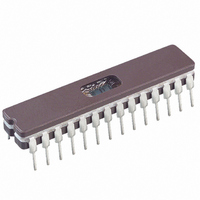
Manufacturer Part Number
PIC18C242/JW
Description
IC MCU EPROM 8KX16 A/D 28CDIP
Manufacturer
Microchip Technology
Series
PIC® 18Cr
Datasheets
1.PIC16F616T-ISL.pdf
(8 pages)
2.PIC16C770-ISO.pdf
(8 pages)
3.PIC18C242-ISO.pdf
(305 pages)
4.PIC18C242-ISO.pdf
(12 pages)
Specifications of PIC18C242/JW
Core Processor
PIC
Core Size
8-Bit
Speed
40MHz
Connectivity
I²C, SPI, UART/USART
Peripherals
Brown-out Detect/Reset, LVD, POR, PWM, WDT
Number Of I /o
22
Program Memory Size
16KB (8K x 16)
Program Memory Type
EPROM, UV
Ram Size
512 x 8
Voltage - Supply (vcc/vdd)
4.2 V ~ 5.5 V
Data Converters
A/D 5x10b
Oscillator Type
External
Operating Temperature
0°C ~ 70°C
Package / Case
28-CDIP (0.300", 7.62mm) Window
Lead Free Status / RoHS Status
Contains lead / RoHS non-compliant
Eeprom Size
-
Available stocks
Company
Part Number
Manufacturer
Quantity
Price
Company:

Part Number:
PIC18C242/JW
Manufacturer:
NS
Quantity:
10


14.3.5
In Slave mode, the data is transmitted and received as
the external clock pulses appear on SCK. When the
last bit is latched, the SSPIF interrupt flag bit is set.
While in Slave mode, the external clock is supplied by
the external clock source on the SCK pin. This external
clock must meet the minimum high and low times as
specified in the electrical specifications.
While in SLEEP mode, the slave can transmit/receive
data. When a byte is received, the device will wake-up
from SLEEP.
14.3.6
The SS pin allows a Synchronous Slave mode. The
SPI must be in Slave mode with SS pin control
enabled (SSPCON1<3:0> = 04h). The pin must not
be driven low for the SS pin to function as an input.
The Data Latch must be high. When the SS pin is
low, transmission and reception are enabled and
the SDO pin is driven. When the SS pin goes high,
FIGURE 14-4:
SS
SCK
(CKP = 0
CKE = 0)
SCK
(CKP = 1
CKE = 0)
Write to
SSPBUF
SDO
SDI
(SMP = 0)
Input
Sample
(SMP = 0)
SSPIF
Interrupt
Flag
SSPSR to
SSPBUF
2001 Microchip Technology Inc.
SLAVE MODE
SLAVE SELECT
SYNCHRONIZATION
SLAVE SYNCHRONIZATION WAVEFORM
bit7
bit7
bit6
the SDO pin is no longer driven, even if in the mid-
dle of a transmitted byte, and becomes a floating
output. External pull-up/pull-down resistors may be
desirable, depending on the application.
When the SPI module resets, the bit counter is forced
to 0. This can be done by either forcing the SS pin to a
high level, or clearing the SSPEN bit.
To emulate two-wire communication, the SDO pin can
be connected to the SDI pin. When the SPI needs to
operate as a receiver, the SDO pin can be configured
as an input. This disables transmissions from the SDO.
The SDI can always be left as an input (SDI function),
since it cannot create a bus conflict.
Note 1: When the SPI is in Slave mode with SS
2: If the SPI is used in Slave mode with CKE
pin control enabled (SSPCON<3:0> =
0100), the SPI module will reset if the SS
pin is set to V
set, then the SS pin control must be
enabled.
bit7
bit7
PIC18CXX2
DD
.
Next Q4 cycle
after Q2
DS39026C-page 125
bit0
bit0
Related parts for PIC18C242/JW
Image
Part Number
Description
Manufacturer
Datasheet
Request
R

Part Number:
Description:
IC, 8BIT MCU, PIC18F, 40MHZ, LCC-44
Manufacturer:
Microchip Technology
Datasheet:
Part Number:
Description:
IC, 8BIT MCU, PIC18LF, 40MHZ, PLCC-64
Manufacturer:
Microchip Technology
Datasheet:
Part Number:
Description:
IC, 8BIT MCU, PIC18F, 64MHZ, TQFP-80
Manufacturer:
Microchip Technology
Datasheet:

Part Number:
Description:
MCU, MPU & DSP Development Tools CAN/LIN PICtail Plus Daughter Board
Manufacturer:
Microchip Technology
Datasheet:

Part Number:
Description:
IC, 8BIT MCU, PIC18F, 64MHZ, DIP-40
Manufacturer:
Microchip Technology
Datasheet:

Part Number:
Description:
IC, 8BIT MCU, PIC18LF, 40MHZ, PLCC-64
Manufacturer:
Microchip Technology
Datasheet:
Part Number:
Description:
IC, 8BIT MCU, PIC18F, 64MHZ, TQFP-64
Manufacturer:
Microchip Technology
Part Number:
Description:
IC, 8BIT MCU, PIC18F, 64MHZ, TQFP-80
Manufacturer:
Microchip Technology

Part Number:
Description:
8KB, Flash, 768bytes-RAM, 36I/O, 8-bit Family,nanowatt XLP 40 UQFN 5x5x0.5mm TUB
Manufacturer:
Microchip Technology
Datasheet:
Part Number:
Description:
8KB, Flash, 768bytes-RAM, 36I/O, 8-bit Family,nanowatt XLP 40 UQFN 5x5x0.5mm TUB
Manufacturer:
Microchip Technology
Part Number:
Description:
16KB, Flash, 768bytes-RAM, 36I/O, 8-bit Family,nanowatt XLP 40 UQFN 5x5x0.5mm TU
Manufacturer:
Microchip Technology
Datasheet:
Part Number:
Description:
16KB, Flash, 768bytes-RAM, 36I/O, 8-bit Family,nanowatt XLP 40 UQFN 5x5x0.5mm TU
Manufacturer:
Microchip Technology
Part Number:
Description:
32KB, Flash, 1536bytes-RAM, 36I/O, 8-bit Family,nanowatt XLP 40 UQFN 5x5x0.5mm T
Manufacturer:
Microchip Technology
Datasheet:
Part Number:
Description:
32KB, Flash, 1536bytes-RAM, 36I/O, 8-bit Family,nanowatt XLP 40 UQFN 5x5x0.5mm T
Manufacturer:
Microchip Technology
Part Number:
Description:
64KB, Flash, 3968bytes-RAM, 36I/O, 8-bit Family,nanowatt XLP 40 UQFN 5x5x0.5mm T
Manufacturer:
Microchip Technology
Datasheet: