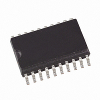
AT90S1200-12YC Atmel, AT90S1200-12YC Datasheet - Page 39

AT90S1200-12YC
Manufacturer Part Number
AT90S1200-12YC
Description
IC MCU 1K FLSH 12MHZ 20SSOP
Manufacturer
Atmel
Series
AVR® 90Sr
Datasheet
1.AT90S1200-12PC.pdf
(71 pages)
Specifications of AT90S1200-12YC
Core Processor
AVR
Core Size
8-Bit
Speed
12MHz
Connectivity
SPI
Peripherals
POR, WDT
Number Of I /o
15
Program Memory Size
1KB (512 x 16)
Program Memory Type
FLASH
Eeprom Size
64 x 8
Voltage - Supply (vcc/vdd)
4 V ~ 6 V
Oscillator Type
Internal
Operating Temperature
0°C ~ 70°C
Package / Case
20-SSOP
Lead Free Status / RoHS Status
Contains lead / RoHS non-compliant
Ram Size
-
Data Converters
-
Available stocks
Company
Part Number
Manufacturer
Quantity
Price
Part Number:
AT90S1200-12YC
Manufacturer:
AT
Quantity:
20 000
Enter Programming Mode
Chip Erase
Programming the Flash
0838H–AVR–03/02
.
Table 15. XA1 and XA0 Coding
Table 16. Command Byte Coding
The following algorithm puts the device in Parallel Programming mode:
1. Apply supply voltage according to Table 13, between V
2. Set the RESET and BS pin to “0” and wait at least 100 ns.
3. Apply 11.5 - 12.5V to RESET. Any activity on BS within 100 ns after +12V has
The Chip Erase command will erase the Flash and EEPROM memories, and the Lock
bits. The Lock bits are not Reset until the Flash and EEPROM have been completely
erased. The Fuse bits are not changed. Chip Erase must be performed before the Flash
or EEPROM is reprogrammed.
Load Command “Chip Erase”
1. Set XA1, XA0 to “10”. This enables command loading.
2. Set BS to “0”.
3. Set DATA to “1000 0000”. This is the command for Chip Erase.
4. Give XTAL1 a positive pulse. This loads the command.
5. Give WR a
A: Load Command “Write Flash”
1. Set XA1, XA0 to “10”. This enables command loading.
2. Set BS to “0”.
3. Set DATA to “0001 0000”. This is the command for Write Flash.
XA1
0
0
1
1
been applied to RESET, will cause the device to fail entering Programming
mode.
in Table 17. Chip Erase does not generate any activity on the RDY/BSY pin.
XA0
0
1
0
1
Command Byte
1000 0000
0100 0000
0010 0000
0001 0000
0001 0001
0000 1000
0000 0100
0000 0010
0000 0011
Action when XTAL1 is Pulsed
Load Flash or EEPROM Address (High or low address byte for Flash
determined by BS).
Load Data (High or low data byte for Flash determined by BS).
Load Command
No Action, Idle
t
WLWH_CE
wide negative pulse to execute Chip Erase,
Read EEPROM
Command Executed
Chip Erase
Write Fuse Bits
Write Lock Bits
Write Flash
Write EEPROM
Read Signature Bytes
Read Fuse and Lock Bits
Read Flash
CC
and GND.
AT90S1200
t
WLWH_CE
is found
39


