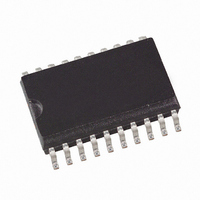
AT90S1200-4YI Atmel, AT90S1200-4YI Datasheet - Page 42

AT90S1200-4YI
Manufacturer Part Number
AT90S1200-4YI
Description
IC MCU 1K FLSH 4MHZ LV IT 20SSOP
Manufacturer
Atmel
Series
AVR® 90Sr
Datasheet
1.AT90S1200-12PC.pdf
(71 pages)
Specifications of AT90S1200-4YI
Core Processor
AVR
Core Size
8-Bit
Speed
4MHz
Connectivity
SPI
Peripherals
POR, WDT
Number Of I /o
15
Program Memory Size
1KB (512 x 16)
Program Memory Type
FLASH
Eeprom Size
64 x 8
Voltage - Supply (vcc/vdd)
2.7 V ~ 6 V
Oscillator Type
Internal
Operating Temperature
-40°C ~ 85°C
Package / Case
20-SSOP
Lead Free Status / RoHS Status
Contains lead / RoHS non-compliant
Ram Size
-
Data Converters
-
Available stocks
Company
Part Number
Manufacturer
Quantity
Price
Part Number:
AT90S1200-4YI
Manufacturer:
ATMEL/爱特梅尔
Quantity:
20 000
Programming the EEPROM
Reading the EEPROM
Programming the Fuse Bits
Programming the Lock Bits
Reading the Fuse and Lock
Bits
42
AT90S1200
The programming algorithm for the EEPROM data memory is as follows (refer to “Pro-
gramming the Flash” for details on command, address and data loading):
1. A: Load Command “0001 0001”.
2. C: Load Address Low Byte ($00 - $3F).
3. D: Load Data Low Byte ($00 - $FF).
4. E: Write Data Low Byte.
The algorithm for reading the EEPROM memory is as follows (refer to “Programming the
Flash” for details on command and address loading):
1. A: Load Command “0000 0011”.
2. C: Load Address Low Byte ($00 - $3F).
3. Set OE to “0”, and BS to “0”. The EEPROM data byte can now be read at DATA.
4. Set OE to “1”.
The algorithm for programming the Fuse bits is as follows (refer to “Programming the
Flash” for details on command and data loading):
1. A: Load Command “0100 0000”.
2. D: Load Data Low Byte. Bit n = “0” programs and bit n = “1” erases the Fuse bit.
3. Give WR a
The algorithm for programming the Lock bits is as follows (refer to “Programming the
Flash” for details on command and data loading):
1. A: Load Command “0010 0000”.
2. D: Load Data Low Byte. Bit n = “0” programs the Lock bit.
3. E: Write Data Low Byte.
The Lock bits can only be cleared by executing Chip Erase.
The algorithm for reading the Fuse and Lock bits is as follows (refer to “Programming
the Flash” on page 39 for details on command loading):
1. A: Load Command “0000 0100”.
2. Set OE to “0”, and BS to “1”. The status of Fuse and Lock bits can now be read
3. Set OE to “1”.
Observe especially that BS needs to be set to “1”.
Bit 5 = SPIEN Fuse
Bit 0 = RCEN Fuse
Bit 7 - 6, 4 - 1 = “1”. These bits are reserved and should be left unprogrammed (“1”).
Bit 2 = Lock Bit2
Bit 1 = Lock Bit1
Bit 7 - 3, 0 = “1”. These bits are reserved and should be left unprogrammed (“1”).
Bit 7 = Lock Bit1
Bit 6 = Lock Bit2
Bit 5 = SPIEN Fuse
Bit 0 = RCEN Fuse
is found in Table 17. Programming the Fuse bits does not generate any activity
on the RDY/BSY pin.
at DATA (“0” means programmed).
t
WLWH_PFB
wide negative pulse to execute the programming;
0838H–AVR–03/02
t
WLWH_PFB


