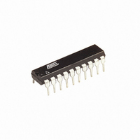
AT90S2313-10PC Atmel, AT90S2313-10PC Datasheet - Page 65

AT90S2313-10PC
Manufacturer Part Number
AT90S2313-10PC
Description
IC MCU 2K FLSH 10MHZ UART 20DIP
Manufacturer
Atmel
Series
AVR® 90Sr
Datasheet
1.AT90S2313-10PC.pdf
(92 pages)
Specifications of AT90S2313-10PC
Core Processor
AVR
Core Size
8-Bit
Speed
10MHz
Connectivity
SPI, UART/USART
Peripherals
Brown-out Detect/Reset, POR, PWM, WDT
Number Of I /o
15
Program Memory Size
2KB (1K x 16)
Program Memory Type
FLASH
Eeprom Size
128 x 8
Ram Size
128 x 8
Voltage - Supply (vcc/vdd)
4 V ~ 6 V
Oscillator Type
External
Operating Temperature
0°C ~ 70°C
Package / Case
20-DIP (0.300", 7.62mm)
Lead Free Status / RoHS Status
Contains lead / RoHS non-compliant
Data Converters
-
Available stocks
Company
Part Number
Manufacturer
Quantity
Price
Company:
Part Number:
AT90S2313-10PC
Manufacturer:
ATM
Quantity:
1 980
Company:
Part Number:
AT90S2313-10PC
Manufacturer:
ATM
Quantity:
1 980
Part Number:
AT90S2313-10PC
Manufacturer:
ATMEL/爱特梅尔
Quantity:
20 000
Part Number:
AT90S2313-10PCS
Manufacturer:
ATMEL/爱特梅尔
Quantity:
20 000
Reading the Flash
Programming the EEPROM
Reading the EEPROM
Programming the Fuse Bits
Programming the Lock Bits
0839I–AVR–06/02
The algorithm for reading the Flash memory is as follows (refer to “Programming the
Flash” for details on command and address loading):
1. A: Load Command “0000 0010”.
2. B: Load Address High Byte ($00 - $03).
3. C: Load Address Low Byte ($00 - $FF).
4. Set OE to “0”, and BS to “0”. The Flash word low byte can now be read at DATA.
5. Set BS to “1”. The Flash word high byte can now be read from DATA.
6. Set OE to “1”.
The programming algorithm for the EEPROM data memory is as follows (refer to “Pro-
gramming the Flash” for details on command, address and data loading):
1. A: Load Command “0001 0001”.
2. C: Load Address Low Byte ($00 - $7F).
3. D: Load Data Low Byte ($00 - $FF).
4. E: Write Data Low Byte.
The algorithm for reading the EEPROM memory is as follows (refer to “Programming the
Flash” for details on command and address loading):
1. A: Load Command “0000 0011”.
2. C: Load Address Low Byte ($00 - $7F).
3. Set OE to “0”, and BS to “0”. The EEPROM data byte can now be read at DATA.
4. Set OE to “1”.
The algorithm for programming the Fuse bits is as follows (refer to “Programming the
Flash” for details on command and data loading):
1. A: Load Command “0100 0000”.
2. D: Load Data Low Byte. Bit n = “0” programs and bit n = “1” erases the Fuse bit.
3. Give WR a
The algorithm for programming the Lock bits is as follows (refer to “Programming the
Flash” on page 63 for details on command and data loading):
1. A: Load Command “0010 0000”.
2. D: Load Data Low Byte. Bit n = “0” programs the Lock bit.
3. E: Write Data Low Byte.
The Lock bits can only be cleared by executing Chip Erase.
Bit 5 = SPIEN Fuse bit.
Bit 0 = FSTRT Fuse bit.
Bit 7 - 6, 4 - 1 = “1”. These bits are reserved and should be left unprogrammed (“1”).
found in Table 26. Programming the Fuse bits does not generate any activity on
the RDY/BSY pin.
Bit 2 = Lock Bit2
Bit 1 = Lock Bit1
Bit 7 - 3, 0 = “1”. These bits are reserved and should be left unprogrammed (“1”).
t
WLWH_PFB
wide negative pulse to execute the programming;
AT90S2313
t
WLWH_PFB
is
65


