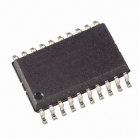
AT90S2313-10SI Atmel, AT90S2313-10SI Datasheet - Page 56

AT90S2313-10SI
Manufacturer Part Number
AT90S2313-10SI
Description
MCU 2K FLASH 10MHZ 20-SOIC
Manufacturer
Atmel
Series
AVR® 90Sr
Datasheet
1.AT90S2313-10PC.pdf
(92 pages)
Specifications of AT90S2313-10SI
Core Processor
AVR
Core Size
8-Bit
Speed
10MHz
Connectivity
SPI, UART/USART
Peripherals
Brown-out Detect/Reset, POR, PWM, WDT
Number Of I /o
15
Program Memory Size
2KB (1K x 16)
Program Memory Type
FLASH
Eeprom Size
128 x 8
Ram Size
128 x 8
Voltage - Supply (vcc/vdd)
4 V ~ 6 V
Oscillator Type
External
Operating Temperature
-40°C ~ 85°C
Package / Case
20-SOIC (7.5mm Width)
Lead Free Status / RoHS Status
Contains lead / RoHS non-compliant
Data Converters
-
Available stocks
Company
Part Number
Manufacturer
Quantity
Price
Company:
Part Number:
AT90S2313-10SI
Manufacturer:
ATMEL
Quantity:
5 510
Part Number:
AT90S2313-10SI
Manufacturer:
ATMEL/爱特梅尔
Quantity:
20 000
Port D Data Register – PORTD
Port D Data Direction Register
– DDRD
Port D Input Pins Address –
PIND
Port D as General Digital I/O
Alternate Functions of Port D
56
AT90S2313
The Port D Input Pins address (PIND) is not a register; this address enables access to
the physical value on each Port D pin. When reading PORTD, the Port D Data Latch is
read, and when reading PIND, the logical values present on the pins are read.
PDn, general I/O pin: The DDDn bit in the DDRD Register selects the direction of this
pin. If DDDn is set (one), PDn is configured as an output pin. If DDDn is cleared (zero),
PDn is configured as an input pin. If PORTDn is set (one) when configured as an input
pin, the MOS pull-up resistor is activated. To switch the pull-up resistor off, the PORTDn
has to be cleared (zero) or the pin has to be configured as an output pin. The Port D pins
are tri-stated when a reset condition becomes active, even if the clock is not active.
Table 20. DDDn Bits on Port D Pins
Note:
The alternate functions of Port D are:
• ICP – Port D, Bit 6
Timer/Counter1 Input Capture pin. See the Timer/Counter1 description for further
details.
• T1 – Port D, Bit 5
T1, Timer 1 Clock source. See the Timer description for further details.
• T0 – Port D, Bit 4
T0, Timer/Counter0 Clock source. See the Timer description for further details.
Bit
$12 ($32)
Read/Write
Initial value
Bit
$11 ($31)
Read/Write
Initial value
Bit
$10 ($30)
Read/Write
Initial value
DDDn
0
0
1
1
1. n: 6…0, pin number.
PORTDn
R
R
R
7
–
0
7
–
0
7
–
0
0
1
0
1
PORTD6
PIND6
DDD6
R/W
R/W
N/A
6
0
6
0
6
R
Output
Output
Input
Input
I/O
PORTD5
PIND5
DDD5
R/W
R/W
N/A
R
5
0
5
0
5
Pull-up
Yes
(1)
No
No
No
PORTD4
PIND4
DDD4
R/W
R/W
N/A
R
4
0
4
0
4
Comment
Tri-state (High-Z)
PDn will source current if ext. pulled low
Push-pull Zero Output
Push-pull One Output
PORTD3
PIND3
DDD3
R/W
R/W
N/A
R
3
0
3
0
3
PORTD2
PIND2
DDD2
R/W
R/W
N/A
2
0
2
0
2
R
PORTD1
PIND1
DDD1
R/W
R/W
N/A
R
1
0
1
0
1
PORTD0
PIND0
DDD0
R/W
R/W
N/A
R
0
0
0
0
0
0839I–AVR–06/02
PORTD
DDRD
PIND


