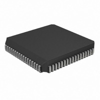
PIC17LC756AT-08/L Microchip Technology, PIC17LC756AT-08/L Datasheet - Page 47

PIC17LC756AT-08/L
Manufacturer Part Number
PIC17LC756AT-08/L
Description
IC MCU OTP 16KX16 A/D 68PLCC
Manufacturer
Microchip Technology
Series
PIC® 17Cr
Specifications of PIC17LC756AT-08/L
Core Processor
PIC
Core Size
8-Bit
Speed
8MHz
Connectivity
I²C, SPI, UART/USART
Peripherals
Brown-out Detect/Reset, POR, PWM, WDT
Number Of I /o
50
Program Memory Size
32KB (16K x 16)
Program Memory Type
OTP
Ram Size
902 x 8
Voltage - Supply (vcc/vdd)
3 V ~ 5.5 V
Data Converters
A/D 12x10b
Oscillator Type
External
Operating Temperature
0°C ~ 70°C
Package / Case
68-PLCC
Processor Series
PIC17LC
Core
PIC
Data Bus Width
8 bit
Data Ram Size
902 B
Interface Type
I2C, MSSP, RS- 232, SCI, SPI, USART
Maximum Clock Frequency
8 MHz
Number Of Programmable I/os
50
Number Of Timers
8
Operating Supply Voltage
3 V to 5.5 V
Maximum Operating Temperature
+ 70 C
Mounting Style
SMD/SMT
Minimum Operating Temperature
0 C
On-chip Adc
12 bit
Data Rom Size
902 B
Height
4.06 mm
Length
24.33 mm
Supply Voltage (max)
5.5 V
Supply Voltage (min)
3 V
Width
24.33 mm
Lead Free Status / RoHS Status
Lead free / RoHS Compliant
Eeprom Size
-
Lead Free Status / Rohs Status
Details
Available stocks
Company
Part Number
Manufacturer
Quantity
Price
Company:
Part Number:
PIC17LC756AT-08/L
Manufacturer:
Microchip Technology
Quantity:
10 000
- Current page: 47 of 304
- Download datasheet (6Mb)
FIGURE 7-5:
Addr
00h
01h
02h
03h
04h
05h
06h
07h
08h
09h
0Ah
0Bh
0Ch
0Dh
0Eh
0Fh
10h
11h
12h
13h
14h
15h
16h
17h
18h
19h
1Ah
1Fh
20h
FFh
Note 1: SFR file locations 10h - 17h are banked. The lower nibble of the BSR specifies the bank. All unbanked
2000 Microchip Technology Inc.
2: General Purpose Registers (GPR) locations 20h - FFh, 120h - 1FFh, 220h - 2FFh, and 320h - 3FFh are
3: RAM bank 3 is not implemented on the PIC17C752 and the PIC17C762. Reading any unimplemented reg-
4: Bank 8 is only implemented on the PIC17C76X devices.
Unbanked
Unbanked
TBLPTRH
TBLPTRL
Bank 0
RCREG1
CPUSTA
TXREG1
SPBRG1
PCLATH
ALUSTA
RCSTA1
TXSTA1
Purpose
Purpose
PRODH
General
General
INTSTA
TMR0H
PORTA
PORTB
PRODL
TMR0L
Bank 0
WREG
T0STA
INDF0
INDF1
DDRB
FSR0
FSR1
SFRs ignore the Bank Select Register (BSR) bits.
banked. The upper nibble of the BSR specifies this bank. All other GPRs ignore the Bank Select Register
(BSR) bits.
ister reads ‘0’s.
RAM
RAM
BSR
PCL
(2)
Bank 1
Bank 1
Purpose
PORTC
PORTD
General
PORTE
DDRC
DDRD
DDRE
PIC17C7XX REGISTER FILE MAP
PIR1
PIE1
RAM
(1)
(2)
PR3H/CA1H
PR3L/CA1L
Bank 2
Bank 2
Purpose
General
TMR3H
TMR3L
TMR1
TMR2
RAM
PR1
PR2
(1)
(2)
Bank 3
PW1DCH
PW2DCH
Bank 3
PW1DCL
PW2DCL
Purpose
General
TCON1
TCON2
CA2H
CA2L
RAM
(2,3)
(1)
Bank 4
RCREG2
SPBRG2
TXREG2
RCSTA2
TXSTA2
PIR2
PIE2
—
(1)
Bank 5
ADCON0
ADCON1
ADRESH
ADRESL
PORTG
PORTF
DDRG
DDRF
(1)
SSPCON1
SSPCON2
SSPSTAT
Bank 6
SSPADD
SSPBUF
—
—
—
PIC17C7XX
(1)
Bank 7
PW3DCH
PW3DCL
TCON3
CA3H
CA4H
CA3L
CA4L
—
DS30289B-page 47
(1)
Bank 8
PORTH
PORTJ
DDRH
DDRJ
—
—
—
—
(1,4)
Related parts for PIC17LC756AT-08/L
Image
Part Number
Description
Manufacturer
Datasheet
Request
R

Part Number:
Description:
MICRO CTRL 16K LOW PWR 68PLCC
Manufacturer:
Microchip Technology
Datasheet:

Part Number:
Description:
MICRO CTRL 16K LOW PWR 64SDIP
Manufacturer:
Microchip Technology
Datasheet:

Part Number:
Description:
MICRO CTRL 16K LOW PWR 64SDIP
Manufacturer:
Microchip Technology
Datasheet:

Part Number:
Description:
MICRO CTRL 16K LOW PWR 68PLCC
Manufacturer:
Microchip Technology
Datasheet:

Part Number:
Description:
Manufacturer:
Microchip Technology Inc.
Datasheet:

Part Number:
Description:
Manufacturer:
Microchip Technology Inc.
Datasheet:

Part Number:
Description:
Manufacturer:
Microchip Technology Inc.
Datasheet:

Part Number:
Description:
Manufacturer:
Microchip Technology Inc.
Datasheet:

Part Number:
Description:
Manufacturer:
Microchip Technology Inc.
Datasheet:

Part Number:
Description:
Manufacturer:
Microchip Technology Inc.
Datasheet:

Part Number:
Description:
Manufacturer:
Microchip Technology Inc.
Datasheet:


