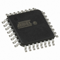
AT90LS4433-4AC Atmel, AT90LS4433-4AC Datasheet - Page 16

AT90LS4433-4AC
Manufacturer Part Number
AT90LS4433-4AC
Description
IC MCU 4K 4MHZ A/D LV 32TQFP
Manufacturer
Atmel
Series
AVR® 90LSr
Datasheet
1.AT90S4433-8AC.pdf
(126 pages)
Specifications of AT90LS4433-4AC
Core Processor
AVR
Core Size
8-Bit
Speed
4MHz
Connectivity
SPI, UART/USART
Peripherals
Brown-out Detect/Reset, POR, PWM, WDT
Number Of I /o
20
Program Memory Size
4KB (2K x 16)
Program Memory Type
FLASH
Eeprom Size
256 x 8
Ram Size
128 x 8
Voltage - Supply (vcc/vdd)
2.7 V ~ 6 V
Data Converters
A/D 6x10b
Oscillator Type
External
Operating Temperature
0°C ~ 70°C
Package / Case
32-TQFP, 32-VQFP
Lead Free Status / RoHS Status
Contains lead / RoHS non-compliant
Available stocks
Company
Part Number
Manufacturer
Quantity
Price
Company:
Part Number:
AT90LS4433-4AC
Manufacturer:
ATM
Quantity:
72
EEPROM Data Memory
Memory Access Times
and Instruction
Execution Timing
16
AT90S/LS4433
The AT90S4433 contains 256 bytes of data EEPROM memory. It is organized as a sep-
arate data space, in which single bytes can be read and written. The EEPROM has an
endurance of at least 100,000 write/erase cycles per location. The access between the
EEPROM and the CPU is described on page 53, specifying the EEPROM Address Reg-
isters, the EEPROM Data Register and the EEPROM Control Register.
For the SPI Data downloading, see page 93 for a detailed description. The EEPROM
Data memory is In-System Programmable through the SPI port. Please refer to the
“EEPROM Read/Write Access” section on page 45 for a thorough description of
EEPROM access.
This section describes the general access timing concepts for instruction execution and
internal memory access.
The AVR CPU is driven by the System Clock Ø, directly generated from the external
clock crystal for the chip. No internal clock division is used.
Figure 21 shows the parallel instruction fetches and instruction executions enabled by
the Harvard architecture and the fast-access Register File concept. This is the basic
pipelining concept to obtain up to 1 MIPS per MHz with the corresponding unique results
for functions per cost, functions per clocks and functions per power unit.
Figure 21. The Parallel Instruction Fetches and Instruction Executions
Figure 22 shows the internal timing concept for the Register File. In a single clock cycle
an ALU operation using two register operands is executed and the result is stored back
to the destination register.
Figure 22. Single Cycle ALU Operation
The internal data SRAM access is performed in two System Clock cycles as described
in Figure 23.
Register Operands Fetch
2nd Instruction Execute
3rd Instruction Execute
1st Instruction Execute
ALU Operation Execute
2nd Instruction Fetch
3rd Instruction Fetch
4th Instruction Fetch
1st Instruction Fetch
Total Execution Time
Result Write Back
System Clock Ø
System Clock Ø
T1
T1
T2
T2
T3
T3
1042H–AVR–04/03
T4
T4


