PIC16C745/JW Microchip Technology, PIC16C745/JW Datasheet - Page 13
PIC16C745/JW
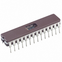
Manufacturer Part Number
PIC16C745/JW
Description
IC MCU EPROM8KX14 USB A/D 28CDIP
Manufacturer
Microchip Technology
Series
PIC® 16Cr
Datasheets
1.PIC16F616T-ISL.pdf
(8 pages)
2.PIC16C745-ISP.pdf
(165 pages)
3.PIC16C745-ISP.pdf
(6 pages)
4.PIC16C745-ISP.pdf
(6 pages)
Specifications of PIC16C745/JW
Core Processor
PIC
Core Size
8-Bit
Speed
24MHz
Connectivity
SCI, UART/USART, USB
Peripherals
Brown-out Detect/Reset, POR, PWM, WDT
Number Of I /o
22
Program Memory Size
14KB (8K x 14)
Program Memory Type
EPROM, UV
Ram Size
256 x 8
Voltage - Supply (vcc/vdd)
4.35 V ~ 5.25 V
Data Converters
A/D 5x8b
Oscillator Type
External
Operating Temperature
0°C ~ 70°C
Package / Case
28-CDIP (0.300", 7.62mm) Window
Lead Free Status / RoHS Status
Contains lead / RoHS non-compliant
Eeprom Size
-
Available stocks
Company
Part Number
Manufacturer
Quantity
Price
Company:

Part Number:
PIC16C745/JW
Manufacturer:
MICROCHIP
Quantity:
51
Part Number:
PIC16C745/JW
Manufacturer:
MICROCHIP/微芯
Quantity:
20 000


3.1
The clock input feeds either an on-chip PLL, or directly
drives (F
direct drive (F
ate four non-overlapping quadrature clocks namely,
Q1, Q2, Q3 and Q4. Internally, the program counter
(PC) is incremented every Q1, the instruction is fetched
from the program memory and latched into the instruc-
tion register in Q4. The instruction is decoded and exe-
cuted during the following Q1 through Q4. The clocks
and instruction execution flow is shown in Figure 3-2.
FIGURE 3-2:
EXAMPLE 3-1:
1. MOVLW 55h
2. MOVWF PORTB
3. CALL
4. BSF
5. Instruction @ address SUB_1
2000 Microchip Technology Inc.
Note:
OSC2/CLKOUT
Clocking Scheme/Instruction Cycle
INT
(EC mode)
). The clock output from either the PLL or
SUB_1
PORTA, BIT3 (Forced NOP)
All instructions are single cycle, except for any program branches. These take two cycles, since the fetch
instruction is “flushed” from the pipeline, while the new instruction is being fetched and then executed.
INT
F
Q1
Q2
Q3
Q4
PC
INT
) is internally divided by four to gener-
CLOCK/INSTRUCTION CYCLE
INSTRUCTION PIPELINE FLOW
Q1
Execute INST (PC-1)
Fetch INST (PC)
Q2
Fetch 1
T
PC
CY
0
Q3
Q4
Execute 1
Fetch 2
T
CY
1
Q1
Preliminary
Execute INST (PC)
Fetch INST (PC+1)
Execute 2
Q2
Fetch 3
T
PC+1
CY
2
3.2
An “Instruction Cycle” consists of four Q cycles (Q1,
Q2, Q3 and Q4). The instruction fetch and execute are
pipelined such that fetch takes one instruction cycle,
while decode and execute takes another instruction
cycle. However, due to the pipelining, each instruction
effectively executes in one cycle. If an instruction
causes the program counter to change (e.g., GOTO),
then two cycles are required to complete the instruction
(Example 3-1).
A fetch cycle begins with the program counter (PC)
incrementing in Q1.
In the execution cycle, the fetched instruction is latched
into the “Instruction Register" (IR) in cycle Q1. This
instruction is then decoded and executed during the
Q2, Q3 and Q4 cycles. Data memory is read during Q2
(operand read) and written during Q4 (destination
write).
Q3
Execute 3
Q4
Fetch 4
Instruction Flow/Pipelining
T
CY
3
Q1
PIC16C745/765
Execute INST (PC+1)
Fetch INST (PC+2)
Fetch SUB_1 Execute SUB_1
Q2
Flush
T
PC+2
CY
4
Q3
Q4
DS41124C-page 13
T
CY
Internal
phase
clock
5
Related parts for PIC16C745/JW
Image
Part Number
Description
Manufacturer
Datasheet
Request
R

Part Number:
Description:
MICRO CTRL 4K 4MHZ OTP 44PLCC
Manufacturer:
Microchip Technology
Datasheet:
Part Number:
Description:
MICRO CTRL 4K 20MHZ OTP 44PLCC
Manufacturer:
Microchip Technology
Datasheet:

Part Number:
Description:
MICRO CTRL 4K 20MHZ OTP 40DIP
Manufacturer:
Microchip Technology
Datasheet:
Part Number:
Description:
MICRO CTRL 4K 10MHZ OTP ET 40DIP
Manufacturer:
Microchip Technology
Datasheet:
Part Number:
Description:
MICRO CTRL 4K 10MHZ OTP 40DIP
Manufacturer:
Microchip Technology
Datasheet:
Part Number:
Description:
MICRO CTRL 4K 4MHZ OTP 40DIP
Manufacturer:
Microchip Technology
Datasheet:
Part Number:
Description:
MICRO CTRL 4K 4MHZ OTP 40DIP
Manufacturer:
Microchip Technology
Datasheet:

Part Number:
Description:
MICRO CTRL 4K 20MHZ EPROM 40CDIP
Manufacturer:
Microchip Technology
Datasheet:

Part Number:
Description:
8-Bit CMOS Microcontrollers with A/D Converter
Manufacturer:
Microchip Technology
Part Number:
Description:
8-Bit CMOS Microcontrollers with A/D Converter
Manufacturer:
Microchip Technology
Part Number:
Description:
8-Bit CMOS Microcontrollers with A/D Converter
Manufacturer:
Microchip Technology
Part Number:
Description:
8-Bit CMOS Microcontrollers with A/D Converter
Manufacturer:
Microchip Technology
Part Number:
Description:
8-Bit CMOS Microcontrollers with A/D Converter
Manufacturer:
Microchip Technology
Part Number:
Description:
8-Bit CMOS Microcontrollers with A/D Converter
Manufacturer:
Microchip Technology
Part Number:
Description:
8-Bit CMOS Microcontrollers with A/D Converter
Manufacturer:
Microchip Technology