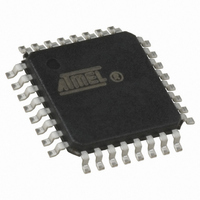
ATTINY28L-4AI Atmel, ATTINY28L-4AI Datasheet - Page 50

ATTINY28L-4AI
Manufacturer Part Number
ATTINY28L-4AI
Description
IC AVR MCU 2KFLSH 4MHZ 3V 32TQFP
Manufacturer
Atmel
Series
AVR® ATtinyr
Specifications of ATTINY28L-4AI
Core Processor
AVR
Core Size
8-Bit
Speed
4MHz
Peripherals
POR, WDT
Number Of I /o
11
Program Memory Size
2KB (1K x 16)
Program Memory Type
FLASH
Voltage - Supply (vcc/vdd)
2.7 V ~ 5.5 V
Oscillator Type
Internal
Operating Temperature
-40°C ~ 85°C
Package / Case
32-TQFP, 32-VQFP
Lead Free Status / RoHS Status
Contains lead / RoHS non-compliant
Eeprom Size
-
Ram Size
-
Data Converters
-
Connectivity
-
Available stocks
Company
Part Number
Manufacturer
Quantity
Price
Part Number:
ATTINY28L-4AI
Manufacturer:
ATMEL/爱特梅尔
Quantity:
20 000
Reading the Flash
Programming the Fuse Bits
Programming the Lock Bits
50
ATtiny28L/V
1. Set BS to “1”. This selects high data.
2. Give WR a negative pulse. This starts programming of the data byte. RDY/BSY
3. Wait until RDY/BSY goes high to program the next byte.
(See Figure 39 for signal waveforms.)
The loaded command and address are retained in the device during programming. For
efficient programming, the following should be considered:
•
•
•
These considerations also apply to Flash and signature bytes reading.
The algorithm for reading the Flash memory is as follows (refer to “Programming the
Flash” for details on command and address loading):
A: Load Command “0000 0010”.
B: Load Address High Byte ($00 - $03).
C: Load Address Low Byte ($00 - $FF).
1. Set OE to “0”, and BS to “0”. The Flash word low byte can now be read at DATA.
2. Set BS to “1”. The Flash word high byte can now be read from DATA.
3. Set OE to “1”.
The algorithm for programming the Fuse bits is as follows (refer to “Programming the
Flash” for details on command and data loading):
A: Load Command “0100 0000”.
D: Load Data Low Byte. Bit n = “0” programs and bit n = “1” erases the Fuse bit.
E: Write Data Low Byte.
The algorithm for programming the Lock bits is as follows (refer to “Programming the
Flash” for details on command and data loading):
A: Load Command “0010 0000”.
D: Load Data Low Byte. Bit n = “0” programs the Lock bit.
E: Write Data Low Byte.
The Lock bits can only be cleared by executing Chip Erase.
goes low.
The command needs to be loaded only once when writing or reading multiple
memory locations.
Address high byte only needs to be loaded before programming a new 256-word
page in the Flash.
Skip writing the data value $FF, that is, the contents of the entire Flash after a Chip
Erase.
Bit 4 = INTCAP Fuse
Bit 3 = CKSEL3 Fuse
Bit 2 = CKSEL2 Fuse
Bit 1 = CKSEL1 Fuse
Bit 0 = CKSEL0 Fuse
Bits 7 - 5 = “1”. These bits are reserved and should be left unprogrammed (“1”).
Bit 2 = Lock Bit2
Bit 1 = Lock Bit1
Bits 7 - 3,0 = “1”. These bits are reserved and should be left unprogrammed (“1”).
1062F–AVR–07/06


