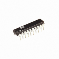
AT89C1051U-24PC Atmel, AT89C1051U-24PC Datasheet

AT89C1051U-24PC
Specifications of AT89C1051U-24PC
Available stocks
Related parts for AT89C1051U-24PC
AT89C1051U-24PC Summary of contents
Page 1
... RAM, 15 I/O lines, two 16-bit timer/counters, a five-vector, two-level interrupt archi- tecture, a full duplex serial port, a precision analog comparator, on-chip oscillator and clock circuitry. In addition, the AT89C1051U is designed with static logic for operation down to zero frequency and supports two software-selectable power saving modes. ...
Page 2
... Block Diagram V CC RAM ADDR. GND REGISTER B REGISTER TIMING INSTRUCTION AND RST REGISTER CONTROL ANALOG COMPARATOR OSC AT89C1051U 2 RAM ACC TMP2 TMP1 ALU INTERRUPT, SERIAL PORT, AND TIMER BLOCKS PSW PORT1 LATCH PORT1 DRIVERS P1.0 - P1.7 FLASH PROGRAM STACK ADDRESS POINTER ...
Page 3
... As inputs, Port 3 pins that are externally being pulled low will source current (I ) because of the pullups. IL Port 3 also serves the functions of various special features of the AT89C1051U as listed below: Port Pin Alternate Functions P3.0 RXD (serial input port) P3.1 TXD (serial output port) P3 ...
Page 4
... Note that not all of the addresses are occupied, and unoc- cupied addresses may not be implemented on the chip. Read accesses to these addresses will in general return random data, and write accesses will have an indetermi- nate effect. Table 1. AT89C1051U SFR Map and Reset Values 0F8H 0F0H B 00000000 ...
Page 5
... MOVX-related instructions, Data Memory: The AT89C1051U contains 64 bytes of internal data mem- ory. Thus, in the AT89C1051U the stack depth is limited to 64 bytes, the amount of available RAM. External DATA memory access is not supported in this device, nor is exter- nal PROGRAM memory execution. Therefore, no MOVX [ ...
Page 6
... P1.0 and P1.1 should be set to “0” external pullups are used, or set to “1” if external pullups are used. Programming The Flash The AT89C1051U is shipped with the 1K byte of on-chip PEROM code memory array in the erased state (i.e., con- tents = FFH) and ready to be programmed. The code memory array is programmed one byte at a time ...
Page 7
... The internal PEROM address counter is reset to 000H on the rising edge of RST and is advanced by a positive pulse at XTAL1 pin. 2. Chip Erase requires a 10-ms PROG pulse. 3. P3.1 is pulled Low during programming to indicate RDY/BSY. Figure 3. Programming the Flash Memory AT89C1051U RST/VPP P3.2/PROG 12V H H Bit - 1 12V Bit - 2 12V 12V H H Figure 4. Verifying the Flash Memory PP AT89C1051U P3.3 P3 AT89C1051U P3 ...
Page 8
... Data Float after ENABLE EHQZ t PROG High to BUSY Low GHBL t Byte Write Cycle Time WC t RDY/BSY to Increment Clock Delay BHIH t Increment Clock High IHIL Flash Programming and Verification Waveforms AT89C1051U 8 PP Min Max Units 11.5 12.5 V 250 µA 1.0 µs 1.0 µs 1.0 µ ...
Page 9
... OL may exceed the related specification. Pins are not guaranteed to sink current greater OL AT89C1051U Stresses beyond those listed under “Absolute Maximum Ratings” may cause permanent dam- age to the device. This is a stress rating only and functional operation of the device at these or any ...
Page 10
... External Clock Drive Waveforms External Clock Drive Symbol Parameter 1/t Oscillator Frequency CLCL t Clock Period CLCL t High Time CHCX t Low Time CLCX t Rise Time CLCH t Fall Time CHCL AT89C1051U 2.7V to 6.0V CC Min Max Min 0 12 83.3 41 4.0V to 6.0V CC Max Units 0 24 ...
Page 11
... Note: 1. For timing purposes, a port pin is no longer floating CC when a 100 mV change from load voltage occurs. A max. for a port pin begins to float when 100 mV change from IL the loaded V AT89C1051U Variable Oscillator Min Max Units 12t µs CLCL 10t -133 ...
Page 12
... Notes: AT89C1051U 12 AT89C1051U TYPICAL ICC - ACTIVE (85˚ Vcc=5. FREQUENCY (MHz) AT89C1051U TYPICAL ICC - IDLE (85˚ Vcc=5. FREQUENCY (MHz) AT89C 1051U TYPICAL ICC vs. VOLTAGE- POWER DOWN (85˚ µ 3.0V 4.0V Vcc VOLTAGE 1. XTAL1 tied to GND for I (power-down P.1.0 and P1 GND CC 3. Lock bits programmed Vcc=6 ...
Page 13
... Power (MHz) Supply Ordering Code 12 2.7V to 6.0V AT89C1051U-12PC AT89C1051U-12SC AT89C1051U-12PI AT89C1051U-12SI 24 4.0V to 6.0V AT89C1051U-24PC AT89C1051U-24SC AT89C1051U-24PI AT89C1051U-24SI 20P3 20-lead, 0.300" Wide, Plastic Dual In-line Package (PDIP) 20S 20-lead, 0.300" Wide, Plastic Gull Wing Small Outline (SOIC) AT89C1051U Package 20P3 20S 20P3 ...
Page 14
... MAX SEATING PLANE .150(3.81) .115(2.92) .070(1.78) .110(2.79) .045(1.13) .090(2.29) 15 .014(.356) .008(.203) .430(10.92) MAX AT89C1051U 14 20S, 20-lead, 0.300" Wide, Plastic Gull Wing Small Outline (SOIC) Dimensions in Inches and (Millimeters) PIN 1 .280(7.11) .240(6.10) .090(2.29) MAX .005(.127) MIN .015(.381) MIN ...
Page 15
... No licenses to patents or other intellectual prop- erty of Atmel are granted by the Company in connection with the sale of Atmel products, expressly or by implication. Atmel’s products are not authorized for use as critical components in life suppor t devices or systems. ...


