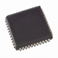
AT87F55WD-24AI Atmel, AT87F55WD-24AI Datasheet - Page 4

AT87F55WD-24AI
Manufacturer Part Number
AT87F55WD-24AI
Description
IC MICRO CTRL 24MHZ 44PLCC
Manufacturer
Atmel
Series
87Fr
Datasheet
1.AT87F55WD-24AC.pdf
(26 pages)
Specifications of AT87F55WD-24AI
Core Processor
8051
Core Size
8-Bit
Speed
24MHz
Connectivity
UART/USART
Peripherals
WDT
Number Of I /o
32
Program Memory Size
20KB (20K x 8)
Program Memory Type
OTP Quick FLASH
Ram Size
256 x 8
Voltage - Supply (vcc/vdd)
4 V ~ 5.5 V
Oscillator Type
Internal
Operating Temperature
-40°C ~ 85°C
Package / Case
44-PLCC
Lead Free Status / RoHS Status
Contains lead / RoHS non-compliant
Eeprom Size
-
Data Converters
-
Other names
AT87F55WD24AI
memory. This pin is also the program pulse input (PROG)
during QuickFlash programming.
In normal operation, ALE is emitted at a constant rate of 1/6
the oscillator frequency and may be used for external
timing or clocking purposes. Note, however, that one
ALE pulse is skipped during each access to external data
memory.
If desired, ALE operation can be disabled by setting bit 0 of
SFR location 8EH. With the bit set, ALE is active only dur-
ing a MOVX or MOVC instruction. Otherwise, the pin is
weakly pulled high. Setting the ALE-disable bit has no
effect if the microcontroller is in external execution mode.
PSEN
Program Store Enable is the read strobe to external pro-
gram memory.
When the AT87F55WD is executing code from external
program memory, PSEN is activated twice each machine
Table 1. AT87F55WD SFR Map and Reset Values
4
0D8H
0D0H
0C8H
0C0H
0E8H
0E0H
0B8H
0B0H
0A8H
0A0H
0F8H
0F0H
98H
90H
88H
80H
XX000000
0X000000
00000000
00000000
00000000
00000000
11111111
11111111
00000000
11111111
00000000
11111111
T2CON
SCON
TCON
PSW
ACC
P3
P2
P1
P0
IP
IE
B
AT87F55WD
XXXXXXXX
XXXXXX00
00000000
00000111
T2MOD
TMOD
SBUF
SP
XXXXXXX0
00000000
00000000
00000000
RCAP2L
AUXR1
DP0L
TL0
00000000
00000000
00000000
RCAP2H
DP0H
TL1
cycle, except that two PSEN activations are skipped during
each access to external data memory.
EA/VPP
External Access Enable. EA must be strapped to GND in
order to enable the device to fetch code from external pro-
gram memory locations starting at 0000H up to FFFFH.
Note, however, that if lock bit 1 is programmed, EA will be
internally latched on reset.
EA should be strapped to V
tions.
This pin also receives the 12-volt programming enable volt-
age (V
XTAL1
Input to the inverting oscillator amplifier and input to the
internal clock operating circuit.
XTAL2
Output from the inverting oscillator amplifier.
00000000
00000000
00000000
DP1L
TH0
TL2
PP
) during QuickFlash programming.
00000000
00000000
00000000
DP1H
TH2
TH1
XXXXXXXX
XXX00XX0
WDTRST
CC
AUXR
for internal program execu-
0XXX0000
PCON
0FFH
0F7H
0EFH
0E7H
0DFH
0D7H
0CFH
0C7H
0BFH
0B7H
0AFH
0A7H
9FH
97H
8FH
87H


