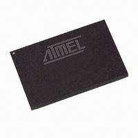
AT91FR4081-33CI Atmel, AT91FR4081-33CI Datasheet - Page 11

AT91FR4081-33CI
Manufacturer Part Number
AT91FR4081-33CI
Description
IC ARM7 MCU 1M FLASH 120 BGA
Manufacturer
Atmel
Series
AT91SAMr
Datasheet
1.AT91FR4081-33CI.pdf
(21 pages)
Specifications of AT91FR4081-33CI
Core Processor
ARM7
Core Size
16/32-Bit
Speed
33MHz
Connectivity
EBI/EMI, UART/USART
Peripherals
WDT
Number Of I /o
32
Program Memory Size
1MB (512K x 16)
Program Memory Type
FLASH
Ram Size
136K x 8
Voltage - Supply (vcc/vdd)
2.7 V ~ 3.6 V
Oscillator Type
External
Operating Temperature
-40°C ~ 85°C
Package / Case
120-BGA
Lead Free Status / RoHS Status
Contains lead / RoHS non-compliant
Eeprom Size
-
Data Converters
-
Other names
AT91FR408133CI
Available stocks
Company
Part Number
Manufacturer
Quantity
Price
Part Number:
AT91FR4081-33CI
Manufacturer:
ATMEL/爱特梅尔
Quantity:
20 000
Abort Control
External Bus Interface
Flash Memory
1386C–ATARM–02/02
The remap command is accessible through the EBI User Interface by writing one in RCB of
EBI_RCR (Remap Control Register). Performing a remap command is mandatory if access to
the other external devices (connected to chip selects 1 to 7) is required. The remap operation
can only be changed back by an internal reset or an NRST assertion.
The abort signal providing a Data Abort or a Prefetch Abort exception to the ARM7TDMI is
asserted when accessing an undefined address in the EBI address space.
No abort is generated when reading the internal memory or by accessing the internal peripher-
als, whether the address is defined or not.
The External Bus Interface handles the accesses between addresses 0x0040 0000 and
0xFFC0 0000. It generates the signals that control access to the external devices, and can be
configured from eight 1-Mbyte banks up to four 16-Mbyte banks. It supports byte, half-word
and word aligned accesses.
For each of these banks, the user can program:
• Number of wait states
• Number of data float times (wait time after the access is finished to prevent any bus
• Data bus width (8-bit or 16-bit)
• With a 16-bit wide data bus, the user can program the EBI to control one 16-bit device (Byte
The External Bus Interface features also the Early Read Protocol, configurable for all the
devices, that significantly reduces access time requirements on an external device in the case
of single-clock cycle access.
In the AT91FR4081, the External Bus Interface connects internally to the Flash memory.
The 8-Mbit Flash memory is organized as 524,288 words of 16 bits each. The Flash memory
is addressed as 16-bit words via the EBI. It uses address lines A1 - A19.
The address, data and control signals, except the Flash memory enable, are internally inter-
connected. The user should connect the Flash memory enable (NCSF) to one of the active-
low chip selects on the EBI; NCS0 must be used if the Flash memory is to be the boot mem-
ory. In addition, if the Flash memory is to be used as boot memory, the BMS input must be
pulled down externally in order for the processor to perform correct 16-bit fetches after reset.
During boot, the EBI must be configured with correct number of standard wait states. For
example, five standard wait states are required when the microcontroller is running at 40 MHz.
The user must ensure that all VDD and all GND pins are connected to their respective sup-
plies by the shortest route. The Flash memory powers-on in the read mode. Command
sequences are used to place the device in other operating modes, such as program and
erase.
A separate Flash memory reset input pin (NRSTF) is provided for maximum flexibility,
enabling the reset operation to adapt to the application. When this input is at a logic high level,
the memory is in its standard operating mode; a low level on this input halts the current mem-
ory operation and puts its outputs in a high impedance state.
The Flash memory features data polling to detect the end of a program cycle. While a program
cycle is in progress, an attempted read of the last word written will return the complement of
the written data on I/O7. An open-drain NBUSY output pin provides another method of detect-
ing the end of a program or erase cycle. This pin is pulled low while program and erase cycles
are in progress and is released at the completion of the cycle. A toggle bit feature provides a
third means of detecting the end of a program or erase cycle.
contention in case the device is too long in releasing the bus)
Access Select Mode) or two 8-bit devices in parallel that emulate a 16-bit memory (Byte
Write Access Mode).
AT91FR4081
11


