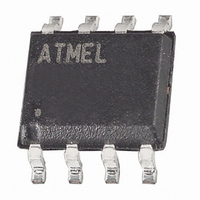
ATTINY12-8SC Atmel, ATTINY12-8SC Datasheet - Page 56

ATTINY12-8SC
Manufacturer Part Number
ATTINY12-8SC
Description
IC AVR MCU 1K 5V 8MHZ COM SO-8
Manufacturer
Atmel
Series
AVR® ATtinyr
Specifications of ATTINY12-8SC
Core Processor
AVR
Core Size
8-Bit
Speed
8MHz
Peripherals
POR, WDT
Number Of I /o
6
Program Memory Size
1KB (512 x 16)
Program Memory Type
FLASH
Eeprom Size
64 x 8
Voltage - Supply (vcc/vdd)
4 V ~ 5.5 V
Oscillator Type
Internal
Operating Temperature
0°C ~ 70°C
Package / Case
8-SOIC (5.3mm Width), 8-SOP, 8-SOEIAJ
Data Bus Width
8 bit
Maximum Clock Frequency
8 MHz
Number Of Programmable I/os
12
Number Of Timers
1 x 8 bit
Operating Supply Voltage
4 V to 5.5 V
Maximum Operating Temperature
+ 85 C
Mounting Style
SMD/SMT
Minimum Operating Temperature
- 55 C
Lead Free Status / RoHS Status
Contains lead / RoHS non-compliant
Ram Size
-
Data Converters
-
Connectivity
-
Lead Free Status / Rohs Status
No
Other names
ATTINY128SC
Available stocks
Company
Part Number
Manufacturer
Quantity
Price
Part Number:
ATTINY12-8SC
Manufacturer:
ATMEL/爱特梅尔
Quantity:
20 000
Data Polling
56
ATtiny11/12
6. Any memory location can be verified by using the Read instruction which returns
7. At the end of the programming session, RESET can be set high to commence
8. Power-off sequence (if needed):
When a byte is being programmed into the Flash or EEPROM, reading the address
location being programmed will give the value $FF. At the time the device is ready for a
new byte, the programmed value will read correctly. This is used to determine when the
next byte can be written. This will not work for the value $FF, so when programming this
value, the user will have to wait for at least t
the next byte. As a chip-erased device contains $FF in all locations, programming of
addresses that are meant to contain $FF can be skipped. This does not apply if the
EEPROM is reprogrammed without chip-erasing the device. In that case, data polling
cannot be used for the value $FF, and the user will have to wait at least t
before programming the next byte. See Table 28 for t
Figure 30. Low-voltage Serial Programming Waveforms
SERIAL DATA OUTPUT
SERIAL CLOCK INPUT
SERIAL DATA INPUT
next instruction. See Table 28 on page 58 for t
an erased device, no $FFs in the data file(s) needs to be programmed.
the content at the selected address at the serial output MISO (PB1) pin.
normal operation.
Set XTAL1 to “0” (if external clocking is used).
Set RESET to “1”.
Turn V
CC
PB0(MOSI)
PB1(MISO)
PB2(SCK)
power off.
MSB
MSB
WD_FLASH
WD_FLASH
or t
WD_FLASH
WD_EEPROM
and t
and t
WD_EEPROM
before programming
WD_EEPROM
1006F–AVR–06/07
values. In
LSB
LSB
WD_EEPROM
values.


