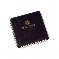
PIC16F871-E/L Microchip Technology, PIC16F871-E/L Datasheet - Page 9

PIC16F871-E/L
Manufacturer Part Number
PIC16F871-E/L
Description
IC MCU CMOS 20MHZ 2K FLSH 44PLCC
Manufacturer
Microchip Technology
Series
PIC® 16Fr
Datasheets
1.PIC16F616T-ISL.pdf
(8 pages)
2.PIC16F688T-ISL.pdf
(688 pages)
3.PIC16F870-ISO.pdf
(172 pages)
4.PIC16F870-ISO.pdf
(6 pages)
Specifications of PIC16F871-E/L
Core Processor
PIC
Core Size
8-Bit
Speed
20MHz
Connectivity
UART/USART
Peripherals
Brown-out Detect/Reset, POR, PWM, WDT
Number Of I /o
33
Program Memory Size
3.5KB (2K x 14)
Program Memory Type
FLASH
Eeprom Size
64 x 8
Ram Size
128 x 8
Voltage - Supply (vcc/vdd)
4 V ~ 5.5 V
Data Converters
A/D 8x10b
Oscillator Type
External
Operating Temperature
-40°C ~ 125°C
Package / Case
44-PLCC
For Use With
DVA16XL441 - ADAPTER DEVICE ICE 44PLCC
Lead Free Status / RoHS Status
Lead free / RoHS Compliant
Available stocks
Company
Part Number
Manufacturer
Quantity
Price
Company:
Part Number:
PIC16F871-E/L
Manufacturer:
Microchip Technology
Quantity:
10 000
TABLE 1-1:
2003 Microchip Technology Inc.
OSC1/CLKI
OSC2/CLKO
MCLR/V
RA0/AN0
RA1/AN1
RA2/AN2/V
RA3/AN3/V
RA4/T0CKI
RA5/AN4
RB0/INT
RB1
RB2
RB3/PGM
RB4
RB5
RB6/PGC
RB7/PGD
RC0/T1OSO/T1CKI
RC1/T1OSI
RC2/CCP1
RC3
RC4
RC5
RC6/TX/CK
RC7/RX/DT
V
V
Legend:
Note 1:
SS
DD
Pin Name
2:
3:
PP
/THV
REF
REF
I = input
OD = Open Drain
This buffer is a Schmitt Trigger input when configured as the external interrupt or LVP mode.
This buffer is a Schmitt Trigger input when used in Serial Programming mode.
This buffer is a Schmitt Trigger input when configured in RC Oscillator mode and a CMOS input otherwise.
-
+
PIC16F870 PINOUT DESCRIPTION
Pin#
8, 19
DIP
10
21
22
23
24
25
26
27
28
12
13
14
15
16
17
18
20
11
9
1
4
5
2
3
6
7
SOIC
Pin#
8, 19
10
21
22
23
24
25
26
27
28
12
13
14
15
16
17
18
20
11
9
1
2
3
4
5
6
7
O = output
— = Not used
I/O/P
Type
I/O
I/O
I/O
I/O
I/O
I/O
I/O
I/O
I/O
I/O
I/O
I/O
I/O
I/O
I/O
I/O
I/O
I/O
I/O
I/O
I/O
I/P
I/O
O
P
P
I
ST/CMOS
TTL/ST
TTL/ST
TTL/ST
TTL/ST
Buffer
ST/OD
Type
TTL
TTL
TTL
TTL
TTL
TTL
TTL
TTL
TTL
ST
ST
ST
ST
ST
ST
ST
ST
ST
—
—
—
I/O = input/output
TTL = TTL input
(1)
(1)
(2)
(2)
(3)
Oscillator crystal input/external clock source input.
Oscillator crystal output. Connects to crystal or resonator in
Crystal Oscillator mode. In RC mode, the OSC2 pin outputs
CLKO, which has 1/4 the frequency of OSC1, and denotes the
instruction cycle rate.
Master Clear (Reset) input or programming voltage input or High
Voltage Test mode control. This pin is an active low RESET to the
device.
PORTA is a bi-directional I/O port.
PORTB is a bi-directional I/O port. PORTB can be software
programmed for internal weak pull-up on all inputs.
PORTC is a bi-directional I/O port.
Ground reference for logic and I/O pins.
Positive supply for logic and I/O pins.
RA0 can also be analog input 0.
RA1 can also be analog input 1.
RA2 can also be analog input 2 or negative analog reference
voltage.
RA3 can also be analog input 3 or positive analog reference
voltage.
RA4 can also be the clock input to the Timer0 module. Output
is open drain type.
RA5 can also be analog input 4.
RB0 can also be the external interrupt pin.
RB3 can also be the low voltage programming input.
Interrupt-on-change pin.
Interrupt-on-change pin.
Interrupt-on-change pin or In-Circuit Debugger pin. Serial
programming clock.
Interrupt-on-change pin or In-Circuit Debugger pin. Serial
programming data.
RC0 can also be the Timer1 oscillator output or Timer1 clock
input.
RC1 can also be the Timer1 oscillator input.
RC2 can also be the Capture1 input/Compare1 output/
PWM1 output.
RC6 can also be the USART Asynchronous Transmit or
Synchronous Clock.
RC7 can also be the USART Asynchronous Receive or
Synchronous Data.
PIC16F870/871
ST = Schmitt Trigger input
P = power
Description
DS30569B-page 7


