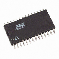
AT89C5131-TISIL Atmel, AT89C5131-TISIL Datasheet - Page 10

AT89C5131-TISIL
Manufacturer Part Number
AT89C5131-TISIL
Description
IC 8051 MCU FLASH 32K USB 28SOIC
Manufacturer
Atmel
Series
AT89C513xr
Datasheet
1.AT89C5131-S3SIL.pdf
(176 pages)
Specifications of AT89C5131-TISIL
Core Processor
C52X2
Core Size
8-Bit
Speed
48MHz
Connectivity
I²C, SPI, UART/USART, USB
Peripherals
LED, POR, PWM, WDT
Number Of I /o
18
Program Memory Size
32KB (32K x 8)
Program Memory Type
FLASH
Eeprom Size
4K x 8
Ram Size
1.25K x 8
Voltage - Supply (vcc/vdd)
3 V ~ 3.6 V
Oscillator Type
Internal
Operating Temperature
-40°C ~ 85°C
Package / Case
28-SOIC (7.5mm Width)
For Use With
AT89STK-10 - KIT EVAL APPL MASS STORAGEAT89STK-05 - KIT STARTER FOR AT89C5131
Lead Free Status / RoHS Status
Contains lead / RoHS non-compliant
Data Converters
-
- Current page: 10 of 176
- Download datasheet (3Mb)
10
AT89C5131
Table 11. System Signal Description
Table 12. Power Signal Description
Signal
AD[7:0]
Signal
A[15:8]
Name
Name
PSEN
AVSS
AVDD
VDD
RST
VSS
ALE
WR
RD
EA
Type
Type
PWR
PWR
GND
GND
I/O
I/O
I/O
I/O
O
O
I
I
Description
Multiplexed Address/Data LSB for external access
Data LSB for Slave port access (used for 8-bit and 16-bit modes)
Address Bus MSB for external access
Data MSB for Slave port access (used for 16-bit mode only)
Read Signal
Read signal asserted during external data memory read operation.
Control input for slave port read access cycles.
Write Signal
Write signal asserted during external data memory write operation.
Control input for slave write access cycles.
Reset Input
Holding this pin low for 64 oscillator periods while the oscillator is running
resets the device. The Port pins are driven to their reset conditions when a
voltage lower than V
This pin has an internal pull-up resistor which allows the device to be reset
by connecting a capacitor between this pin and VSS.
Asserting RST when the chip is in Idle mode or Power-down mode returns
the chip to normal operation.
This pin is set to 0 for at least 12 oscillator periods when an internal reset
occurs.
Address Latch Enable Output
The falling edge of ALE strobes the address into external latch. This signal
is active only when reading or writing external memory using MOVX
instructions.
Program
Test mode entry signal. This pin must be set to V
External Access Enable
This pin must be held low to force the device to fetch code from external
program memory starting at address 0000h. It is latched during reset and
cannot be dynamically changed during operation.
Description
Alternate Ground
AVSS is used to supply the on-chip PLL and the USB PAD.
Alternate Supply Voltage
AVDD is used to supply the on-chip PLL and the USB PAD.
Digital Ground
VSS is used to supply the buffer ring and the digital core.
Digital Supply Voltage
VDD is used to supply the buffer ring on all versions of the device.
It is also used to power the on-chip voltage regulator of the Standard
versions or the digital core of the Low Power versions.
IL
is applied, whether or not the oscillator is running.
DD
for normal operation.
4136B–USB–09/03
Alternate
Alternate
Function
Function
P0[7:0]
P2[7:0]
P3.7
P3.6
-
-
-
-
-
-
-
-
Related parts for AT89C5131-TISIL
Image
Part Number
Description
Manufacturer
Datasheet
Request
R

Part Number:
Description:
8-bit Flash Microcontroller With Full Speed Usb Device At89c5131
Manufacturer:
ATMEL Corporation
Datasheet:

Part Number:
Description:
IC 8051 MCU FLASH 32K USB 52PLCC
Manufacturer:
Atmel
Datasheet:

Part Number:
Description:
8-bit Flash Microcontroller with Full Speed USB Device
Manufacturer:
ATMEL Corporation
Datasheet:

Part Number:
Description:
KIT STARTER FOR AT89C5131
Manufacturer:
Atmel
Datasheet:

Part Number:
Description:
IC 8051 MCU FLASH 32K USB 48QFN
Manufacturer:
Atmel
Datasheet:

Part Number:
Description:
IC 8051 MCU FLASH 32K USB 64VQFP
Manufacturer:
Atmel
Datasheet:

Part Number:
Description:
DEV KIT FOR AVR/AVR32
Manufacturer:
Atmel
Datasheet:

Part Number:
Description:
INTERVAL AND WIPE/WASH WIPER CONTROL IC WITH DELAY
Manufacturer:
ATMEL Corporation
Datasheet:

Part Number:
Description:
Low-Voltage Voice-Switched IC for Hands-Free Operation
Manufacturer:
ATMEL Corporation
Datasheet:

Part Number:
Description:
MONOLITHIC INTEGRATED FEATUREPHONE CIRCUIT
Manufacturer:
ATMEL Corporation
Datasheet:

Part Number:
Description:
AM-FM Receiver IC U4255BM-M
Manufacturer:
ATMEL Corporation
Datasheet:

Part Number:
Description:
Monolithic Integrated Feature Phone Circuit
Manufacturer:
ATMEL Corporation
Datasheet:

Part Number:
Description:
Multistandard Video-IF and Quasi Parallel Sound Processing
Manufacturer:
ATMEL Corporation
Datasheet:


