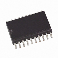
ATAM893T-TKQ Atmel, ATAM893T-TKQ Datasheet - Page 30

ATAM893T-TKQ
Manufacturer Part Number
ATAM893T-TKQ
Description
IC MON TIRE-PRESS ATARX9X SER
Manufacturer
Atmel
Series
MARC4r
Datasheet
1.ATAM893T-TKS.pdf
(98 pages)
Specifications of ATAM893T-TKQ
Core Processor
MARC4
Core Size
4-Bit
Speed
4MHz
Connectivity
SSI (2-Wire, 3 Wire)
Peripherals
Brown-out Detect/Reset, POR, PWM, WDT
Number Of I /o
16
Program Memory Size
4KB (4K x 8)
Program Memory Type
EEPROM
Eeprom Size
64 x 16
Ram Size
256 x 4
Voltage - Supply (vcc/vdd)
1.8 V ~ 6.5 V
Oscillator Type
Internal
Operating Temperature
-40°C ~ 125°C
Package / Case
20-SOIC (5.3mm Width), 20-SO, 20-SOEIAJ
Lead Free Status / RoHS Status
Contains lead / RoHS non-compliant
Data Converters
-
5.2.4.1
5.2.4.2
Table 5-4.
5.2.5
30
Auxiliary Address: '4'hex First Write Cycle
3 2 1 0
x x 1 1
x x 1 0
x x 0 1
x x 0 0
1 1 x x
1 0 x x
0 1 x x
0 0 x x
Code
ATAM893-D
Function
BP40 in input mode
BP40 in output mode
BP40 enable alternate function (SC for SSI)
BP40 enable alternate function (falling edge interrupt
input for INT3)
BP41 in input mode
BP41 in output mode
BP41 enable alternate function
(VMI for voltage monitor input)
BP41 enable alternate function
(T2I external clock input for Timer 2)
Bi-directional Port 6
Port 4 Data Register (P4DAT)
Port 4 Control Register (P4CR) Byte Write
Port 4 Control Register
P4xM2, P4xM1
The bi-directional Port 6 is a bit-wise configurable I/O port and provides the external pins for the
Timer 3. As a normal port, it performs in exactly the same way as bi-directional Port 6 (see
ure 5-6 on page
passed over to other internal modules (Timer 3). The I/O pin for the T3I line has an additional
mode to generate a Timer 3-interrupt.
All two Port 6 pins can be individually switched by the P6CR register.
shows the internal interfaces to bi-directional Port 6.
P4CR
P4DAT
First write cycle
Second write
cycle
Bit 3
P4DAT3
–
Port 4x Interrupt Mode/Direction Code
29). Two additional multiplexes allow data and port direction control to be
Bit 2
P4DAT2
Bit 3
P41M2
Bit 7
P43M2
Second Write Cycle
3 2 1 0
x x 1 1
x x 1 0
1 1 x x
1 0 x x
0 1 x x
0 0 x x
x x 0 x
Code
Bit 1
P4DAT1
–
Bit 2
P41M1
Bit 6
P43M1
Function
BP43 in input mode
BP43 enable alternate function (SD for SSI)
BP42 in input mode
BP42 in output mode
BP42 enable alternate function (T2O for Timer 2)
BP43 in output mode
BP43 enable alternate function (falling edge interrupt
input for INT3)
–
Bit 0
P4DAT0
Bit 1
P40M2
Bit 5
P42M2
Auxiliary register address: '4'hex
Bit 0
P40M1
Bit 4
P42M1
Primary register address: '4'hex
Reset value: 1111b
Reset value: 1111b
Reset value: 1111b
Figure 5-6 on page 29
4680C–4BMCU–01/05
Fig-


