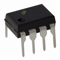
ACE1501EN Fairchild Semiconductor, ACE1501EN Datasheet - Page 22

ACE1501EN
Manufacturer Part Number
ACE1501EN
Description
IC MCU 1KBIT EEPROM 8DIP
Manufacturer
Fairchild Semiconductor
Series
ACEX® 15xxr
Datasheet
1.ACE1501EN.pdf
(33 pages)
Specifications of ACE1501EN
Core Processor
ACE1502
Core Size
8-Bit
Speed
25MHz
Peripherals
Brown-out Detect/Reset, LVD, POR, PWM, WDT
Number Of I /o
6
Program Memory Size
1KB (1K x 8)
Program Memory Type
EEPROM
Eeprom Size
64 x 8
Ram Size
64 x 8
Voltage - Supply (vcc/vdd)
1.8 V ~ 3.6 V
Oscillator Type
Internal
Operating Temperature
-40°C ~ 85°C
Package / Case
8-DIP (0.300", 7.62mm)
Lead Free Status / RoHS Status
Lead free / RoHS Compliant
Data Converters
-
Connectivity
-
ACE1501 Product Family Rev. 1.1
Figure 27. Multi-input Wakeup (MIW) Block Diagram
10.
9. I/O Port
The eight I/O pins (six on 8-pin package option) are bi-
directional (see Figure 28). The bi-directional I/O pins can be
individually configured by software to operate as high-
impedance inputs, as inputs with weak pull-up, or as push-pull
outputs. The operating state is determined by the contents of
the corresponding bits in the data and configuration registers.
Each bi-directional I/O pin can be used for general purpose I/O,
or in some cases, for a specific alternate function determined by
the on-chip hardware.
Figure 28. PORTGD Logic Diagram
Figure 29. I/O Register bit assignments
11. Available only on the 14-pin package option
12. G3 after reset is an input with weak pull-up
Table 13. I/O configuration options
Configuration Bit
GXPULLEN
Bit 7
GXBUFEN
11
WKINTEN: Bit 7 of T0CNTRL
G7
GXOUT
GXIN
0
0
1
1
G0
G7
Bit 6
11
WKEDG[0:7]
G6
7
Bit 5
Data Bit
WKEN[7:0]
G5
0
1
0
1
Data Bus
PORTGC, PORTGD, PORTGD
0
Bit 4
GX
G4
High-impedence input (TRI-STATE input)
Input with pull-up (weak one input)
Push-pull zero output
Push-pull one output
WKPND[0:7]
22
0
7
9.1 I/O registers
The I/O pins (G0-G7) have three memory-mapped port regis-
ters associated with the I/O circuitry: a port configuration regis-
ter (PORTGC), a port data register (PORTGD), and a port input
register (PORTGP). PORTGC is used to configure the pins as
inputs or outputs. A pin may be configured as an input by writing
a 0 or as an output by writing a 1 to its corresponding PORTGC
bit. If a pin is configured as an output, its PORTGD bit repre-
sents the state of the pin (1 = logic high, 0 = logic low). If the pin
is configured as an input, its PORTGD bit selects whether the
pin is a weak pull-up or a high-impedance input. Table 13 pro-
vides details of the port configuration options. The port configu-
ration and data registers can both be read from or written to.
Reading PORTGP returns the value of the port pins regardless
of how the pins are configured. Since this device supports MIW,
PORTG inputs have Schmitt triggers.
Bit 3
12
G3
WKINTEN
Port Pin Configuration
10
Bit 2
G2
Bit 1
G1
WKOUT
EDGEI
www.fairchildsemi.com
Bit 0
G0


