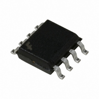
ACE1202LEM8X Fairchild Semiconductor, ACE1202LEM8X Datasheet - Page 30

ACE1202LEM8X
Manufacturer Part Number
ACE1202LEM8X
Description
IC MCU 2KBIT EEPROM 8SOIC
Manufacturer
Fairchild Semiconductor
Series
ACEX® 12xxr
Datasheet
1.ACE1202EMX.pdf
(39 pages)
Specifications of ACE1202LEM8X
Core Processor
ACE1202
Core Size
8-Bit
Speed
4MHz
Peripherals
Brown-out Detect/Reset, LVD, POR, PWM, WDT
Number Of I /o
6
Program Memory Size
2KB (2K x 8)
Program Memory Type
EEPROM
Eeprom Size
64 x 8
Ram Size
64 x 8
Voltage - Supply (vcc/vdd)
1.8 V ~ 5.5 V
Oscillator Type
Internal
Operating Temperature
-40°C ~ 85°C
Package / Case
8-SOIC (3.9mm Width)
Lead Free Status / RoHS Status
Lead free / RoHS Compliant
Data Converters
-
Connectivity
-
ACE1202 Product Family Rev. B.1
The ACEx microcontroller supports in-circuit programming of the
internal data EEPROM, code EEPROM, and the initialization registers.
An externally controlled four wire interface consisting of a LOAD
control pin (G3), a serial data SHIFT-IN input pin (G4), a serial data
SHIFT-OUT output pin (G2), and a CLOCK pin (G1) is used to access
the on-chip memory locations. Communication between the ACEx
microcontroller and the external programmer is made through a 32-
bit command and response word described in Table 15.
The serial data timing for the four-wire interface is shown in Figure
31 and the programming protocol is shown in Figure 30.
The external programmer brings the ACEx microcontroller into
programming mode by applying a super voltage level to the LOAD
pin. The external programmer then needs to set the LOAD pin to 5V
before shifting in the 32-bit serial command word using the SHIFT_IN
and CLOCK signals. By definition, bit 31 of the command word is
shifted in first. At the same time, the ACEx microcontroller shifts out
the 32-bit serial response to the last command on the SHIFT_OUT
pin. It is recommended that the external programmer samples this
signal t
The serial response word, sent immediately after entering program-
ming mode, contains indeterminate data.
After 32 bits have been shifted into the device, the external
programmer must set the LOAD signal to 0V, and then apply two
clock pulses as shown in Figure 30 to complete program cycle.
The SHIFT_OUT pin acts as the handshaking signal between the
device and programming hardware once the LOAD signal is
brought low. The device sets SHIFT_OUT low by the time the
programmer has sent the second rising edge during the LOAD =
15
16
For further information see Application Note AN-8005.
During in-circuit programming, G5 must be either not connected or driven high.
ACCESS
(500ns) after the rising edge of the CLOCK signal.
Must be set to 0
Set to 1 to read/write data EEPROM, or the
initialization registers, otherwise 0
Set to 1 to read/write code EEPROM,
otherwise 0
Must be set to 0
Set to 1 to read, 0 to write
Must be set to 0
Address of the byte to be read or written
Data to be programm ed or zero if data is to be read
0V phase (if the timing specifications in Figure 30 are obeyed).
The device will set the R bit of the Status register when the write
operation has completed. The external programmer must wait for
the SHIFT_OUT pin to go high before bringing the LOAD signal to
5V to initiate a normal command cycle.
When reading the device after a write, the external programmer
must set the LOAD signal to 5V before it sends the new command
word. Next, the 32-bit serial command word (for during a READ)
should be shifted into the device using the SHIFT_IN and the
CLOCK signals while the data from the previous command is
serially shifted out on the SHIFT_OUT pin. After the Read com-
mand has been shifted into the device, the external programmer
must, once again, set the LOAD signal to 0V and apply two clock
pulses as shown in Figure 30 to complete READ cycle. Data from
the selected memory location, will be latched into the lower 8 bits
of the command word shortly after the second rising edge of the
CLOCK signal.
Writing a series of bytes to the device is achieved by sending a
series of Write command words while observing the devices
handshaking requirements.
Reading a series of bytes from the device is achieved by sending
a series of Read command words with the desired addresses in
sequence and reading the following response words to verify the
correct address and data contents.
The addresses of the data EEPROM and code EEPROM loca-
tions are the same as those used in normal operation.
Powering down the device will cause the part to exit programming
mode.
X
X
X
X
X
X
Same as Input command word
Programmed data or data read at specified address
www.fairchildsemi.com


