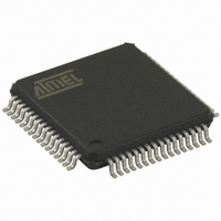
TS87C51RD2-MCM Atmel, TS87C51RD2-MCM Datasheet - Page 54

TS87C51RD2-MCM
Manufacturer Part Number
TS87C51RD2-MCM
Description
IC MCU 8051 OTP 64K 5V 64VQFP
Manufacturer
Atmel
Series
87Cr
Specifications of TS87C51RD2-MCM
Core Processor
8051
Core Size
8-Bit
Speed
40/20MHz
Connectivity
UART/USART
Peripherals
POR, PWM, WDT
Number Of I /o
48
Program Memory Size
64KB (64K x 8)
Program Memory Type
OTP
Ram Size
1K x 8
Voltage - Supply (vcc/vdd)
4.5 V ~ 5.5 V
Oscillator Type
Internal
Operating Temperature
0°C ~ 70°C
Package / Case
64-TQFP, 64-VQFP
Lead Free Status / RoHS Status
Lead free / RoHS Compliant
Eeprom Size
-
Data Converters
-
Available stocks
Company
Part Number
Manufacturer
Quantity
Price
TS80C51RA2/RD2
TS83C51RB2/RC2/RD2
TS87C51RB2/RC2/RD2
8.3.3. Programming Algorithm
The Improved Quick Pulse algorithm is based on the Quick Pulse algorithm and decreases the number of pulses
applied during byte programming from 25 to 1.
To program the TS87C51RB2/RC2/RD2 the following sequence must be exercised:
Repeat step 2 through 6 changing the address and data for the entire array or until the end of the object file is
reached (See Figure 19.).
8.3.4. Verify algorithm
Code array verify must be done after each byte or block of bytes is programmed. In either case, a complete verify
of the programmed array will ensure reliable programming of the TS87C51RB2/RC2/RD2.
P 2.7 is used to enable data output.
To verify the TS87C51RB2/RC2/RD2 code the following sequence must be exercised:
Repeat step 2 through 3 changing the address for the entire array verification (See Figure 19.)
The encryption array cannot be directly verified. Verification of the encryption array is done by observing that the
code array is well encrypted.
54
* See Table 31. for proper value on these inputs
Step 1: Activate the combination of control signals.
Step 2: Input the valid address on the address lines.
Step 3: Input the appropriate data on the data lines.
Step 4: Raise EA/VPP from VCC to VPP (typical 12.75V).
Step 5: Pulse ALE/PROG once.
Step 6: Lower EA/VPP from VPP to VCC
Step 1: Activate the combination of program and control signals.
Step 2: Input the valid address on the address lines.
Step 3: Read data on the data lines.
PROGRAM
SIGNALS*
CONTROL
SIGNALS*
4 to 6 MHz
Figure 18. Set-Up Modes Configuration
PSEN
P2.6
P2.7
P3.3
P3.6
P3.7
XTAL1
EA/VPP
ALE/PROG
RST
P0.0-P0.7
P1.0-P1.7
P2.0-P2.5
P3.4-P3.5
VCC
VSS
GND
+5V
D0-D7
A0-A7
A8-A15
Rev. C - 06 March, 2001


