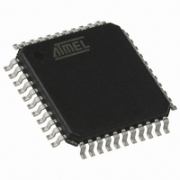
TS80C32X2-VCED Atmel, TS80C32X2-VCED Datasheet - Page 34

TS80C32X2-VCED
Manufacturer Part Number
TS80C32X2-VCED
Description
IC 8051 MCU ROMLESS 5V 44VQFP
Manufacturer
Atmel
Series
80Cr
Datasheet
1.TS87C52X2-VCA.pdf
(55 pages)
Specifications of TS80C32X2-VCED
Core Processor
8051
Core Size
8-Bit
Speed
60/30MHz
Connectivity
UART/USART
Peripherals
POR
Number Of I /o
32
Program Memory Type
ROMless
Ram Size
256 x 8
Voltage - Supply (vcc/vdd)
4.5 V ~ 5.5 V
Oscillator Type
Internal
Operating Temperature
0°C ~ 70°C
Package / Case
44-TQFP, 44-VQFP
Lead Free Status / RoHS Status
Contains lead / RoHS non-compliant
Eeprom Size
-
Program Memory Size
-
Data Converters
-
Available stocks
Company
Part Number
Manufacturer
Quantity
Price
Programming Algorithm
Verify Algorithm
Figure 12. Programming and Verification Signal’s Waveform
EPROM Erasure
(Windowed Packages
Only)
Erasure Characteristics
34
TS8xCx2X2
C o n t r o l s i g n a l s
A L E / P R O G
E A / V P P
A 0 - A 1 2
D 0 - D 7
1 2 . 7 5 V
5 V
0 V
The Improved Quick Pulse algorithm is based on the Quick Pulse algorithm and
decreases the number of pulses applied during byte programming from 25 to 1.
To program the TS87C52X2 the following sequence must be exercised:
•
•
•
•
•
•
Repeat step 2 through 6 changing the address and data for the entire array or until the
end of the object file is reached (See Figure 12.).
Code array verify must be done after each byte or block of bytes is programmed. In
either case, a complete verify of the programmed array will ensure reliable programming
of the TS87C52X2.
P 2.7 is used to enable data output.
To verify the TS87C52X2 code the following sequence must be exercised:
•
•
•
Repeat step 2 through 3 changing the address for the entire array verification (See Fig-
ure 12.)
The encryption array cannot be directly verified. Verification of the encryption array is
done by observing that the code array is well encrypted.
Erasing the EPROM erases the code array, the encryption array and the lock bits return-
ing the parts to full functionality.
Erasure leaves all the EPROM cells in a 1’s state (FF).
The recommended erasure procedure is exposure to ultraviolet light (at 2537 Å) to an
integrated dose at least 15 W-sec/cm
P r o g r a m m i n g C y c l e
Step 1: Activate the combination of control signals.
Step 2: Input the valid address on the address lines.
Step 3: Input the appropriate data on the data lines.
Step 4: Raise EA/VPP from VCC to VPP (typical 12.75V).
Step 5: Pulse ALE/PROG once.
Step 6: Lower EA/VPP from VPP to VCC
Step 1: Activate the combination of program and control signals.
Step 2: Input the valid address on the address lines.
Step 3: Read data on the data lines.
D a t a I n
1 0 0
μ
s
R e a d / V e r i f y C y c l e
2
. Exposing the EPROM to an ultraviolet lamp of
D a t a O u t
4184G–8051–09/06


