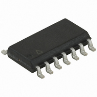
ATTINY44V-10SSU Atmel, ATTINY44V-10SSU Datasheet - Page 138

ATTINY44V-10SSU
Manufacturer Part Number
ATTINY44V-10SSU
Description
IC MCU AVR 4K FLASH 10MHZ 14SOIC
Manufacturer
Atmel
Series
AVR® ATtinyr
Specifications of ATTINY44V-10SSU
Core Processor
AVR
Core Size
8-Bit
Speed
10MHz
Connectivity
USI
Peripherals
Brown-out Detect/Reset, POR, PWM, WDT
Number Of I /o
12
Program Memory Size
4KB (2K x 16)
Program Memory Type
FLASH
Eeprom Size
256 x 8
Ram Size
256 x 8
Voltage - Supply (vcc/vdd)
1.8 V ~ 5.5 V
Data Converters
A/D 8x10b
Oscillator Type
Internal
Operating Temperature
-40°C ~ 85°C
Package / Case
14-SOIC (3.9mm Width), 14-SOL
Package
14SOIC
Device Core
AVR
Family Name
ATtiny
Maximum Speed
10 MHz
Operating Supply Voltage
2.5|3.3|5 V
Data Bus Width
8 Bit
Number Of Programmable I/os
12
Interface Type
SPI/USI
On-chip Adc
8-chx10-bit
Number Of Timers
2
For Use With
ATAVRISP2 - PROGRAMMER AVR IN SYSTEM
Lead Free Status / RoHS Status
Lead free / RoHS Compliant
Available stocks
Company
Part Number
Manufacturer
Quantity
Price
Part Number:
ATTINY44V-10SSU
Manufacturer:
ATMEL/爱特梅尔
Quantity:
20 000
- Current page: 138 of 238
- Download datasheet (5Mb)
16.6
16.6.1
138
Changing Channel or Reference Selection
ATtiny24/44/84
ADC Input Channels
For a summary of conversion times, see
Table 16-1.
The MUX5:0 and REFS1:0 bits in the ADMUX Register are single buffered through a temporary
register to which the CPU has random access. This ensures that the channels and reference
selection only takes place at a safe point during the conversion. The channel and reference
selection is continuously updated until a conversion is started. Once the conversion starts, the
channel and reference selection is locked to ensure a sufficient sampling time for the ADC. Con-
tinuous updating resumes in the last ADC clock cycle before the conversion completes (ADIF in
ADCSRA is set). Note that the conversion starts on the following rising ADC clock edge after
ADSC is written. The user is thus advised not to write new channel or reference selection values
to ADMUX until one ADC clock cycle after ADSC is written.
If Auto Triggering is used, the exact time of the triggering event can be indeterministic. Special
care must be taken when updating the ADMUX Register, in order to control which conversion
will be affected by the new settings.
If both ADATE and ADEN is written to one, an interrupt event can occur at any time. If the
ADMUX Register is changed in this period, the user cannot tell if the next conversion is based
on the old or the new settings. ADMUX can be safely updated in the following ways:
When updating ADMUX in one of these conditions, the new settings will affect the next ADC
conversion.
When changing channel selections, the user should observe the following guidelines to ensure
that the correct channel is selected:
In Single Conversion mode, always select the channel before starting the conversion. The chan-
nel selection may be changed one ADC clock cycle after writing one to ADSC. However, the
simplest method is to wait for the conversion to complete before changing the channel selection.
In Free Running mode, always select the channel before starting the first conversion. The chan-
nel selection may be changed one ADC clock cycle after writing one to ADSC. However, the
simplest method is to wait for the first conversion to complete, and then change the channel
Condition
First conversion
Normal conversions
Auto Triggered conversions
Free Running conversion
• When ADATE or ADEN is cleared.
• During conversion, minimum one ADC clock cycle after the trigger event.
• After a conversion, before the Interrupt Flag used as trigger source is cleared.
ADC Conversion Time
Sample & Hold (Cycles from
Start of Conversion)
Table
13.5
1.5
2.5
2
16-1.
Conversion Time (Cycles)
13.5
25
13
14
8006K–AVR–10/10
Related parts for ATTINY44V-10SSU
Image
Part Number
Description
Manufacturer
Datasheet
Request
R

Part Number:
Description:
Manufacturer:
ATMEL Corporation
Datasheet:

Part Number:
Description:
MCU AVR 4K FLASH 15MHZ 20-QFN
Manufacturer:
Atmel
Datasheet:

Part Number:
Description:
IC MCU AVR 4K FLASH 10MHZ 20-QFN
Manufacturer:
Atmel
Datasheet:

Part Number:
Description:
MCU AVR 4KB FLASH 10MHZ 20SOIC
Manufacturer:
Atmel
Datasheet:

Part Number:
Description:
MCU AVR 4KB FLASH 10MHZ 32QFN
Manufacturer:
Atmel
Datasheet:

Part Number:
Description:
IC MCU AVR 4K FLASH 10MHZ 14-DIP
Manufacturer:
Atmel
Datasheet:

Part Number:
Description:
Manufacturer:
Atmel Corporation
Datasheet:

Part Number:
Description:
Manufacturer:
Atmel Corporation
Datasheet:

Part Number:
Description:
MCU AVR 4K FLASH 15MHZ 20-QFN
Manufacturer:
Atmel
Datasheet:

Part Number:
Description:
IC MCU AVR 4K FLASH 20MHZ 20-QFN
Manufacturer:
Atmel
Datasheet:

Part Number:
Description:
IC MCU AVR 4K FLASH 20MHZ 14SOIC
Manufacturer:
Atmel
Datasheet:


